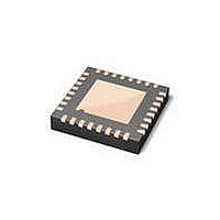
ISP1504CBS NXP Semiconductors, ISP1504CBS Datasheet - Page 16

ISP1504CBS
Manufacturer Part Number
ISP1504CBS
Description
RF Transceiver USB2.0 ULPI OTG TRANSCEIVER
Manufacturer
NXP Semiconductors
Datasheet
1.ISP1504ABS118.pdf
(83 pages)
Specifications of ISP1504CBS
Operating Supply Voltage
1.65 V to 3.6 V
Mounting Style
SMD/SMT
Package / Case
HVQFN
Minimum Operating Temperature
- 40 C
Lead Free Status / RoHS Status
Lead free / RoHS Compliant
Other names
ISP1504CBS,157
Available stocks
Company
Part Number
Manufacturer
Quantity
Price
Part Number:
ISP1504CBS
Manufacturer:
NXP/恩智浦
Quantity:
20 000
Company:
Part Number:
ISP1504CBSFA
Manufacturer:
NXP
Quantity:
6 041
NXP Semiconductors
8. Modes of operation
ISP1504A_ISP1504C_3
Product data sheet
8.1.1 Synchronous mode
8.1 ULPI modes
The ISP1504 ULPI bus can be programmed to operate in four modes. Each mode
reconfigures the signals on the data bus as described in the following subsections. Setting
more than one mode will lead to undefined behavior.
This is default mode. At power-up, and when CLOCK is stable, the ISP1504 will enter
synchronous mode. The link must synchronize all ULPI signals to CLOCK, meeting the
set-up and hold times as defined in
synchronous mode is given in
This mode is used by the link to perform the following tasks:
For more information on various synchronous mode protocols, see
Table 4.
Signal
name
CLOCK
DATA[7:0] I/O
•
•
•
•
High-speed detection handshake (chirp)
Transmit and receive USB packets
Read and write to registers
Receive USB status updates (RXCMDs)
ULPI signal description
Direction
on ISP1504
O
Rev. 03 — 7 April 2008
Signal description
60 MHz interface clock. If a crystal is attached or a clock is driven into
the XTAL1 pin, the ISP1504 will drive a 60 MHz output clock.
8-bit data bus. In synchronous mode, the link drives DATA[7:0] to LOW
by default. The link initiates transfers by sending a nonzero data pattern
called TXCMD (transmit command). In synchronous mode, the direction
of DATA[7:0] is controlled by DIR. Contents of DATA[7:0] lines must be
ignored for exactly one clock cycle whenever DIR changes value. This is
called the turnaround cycle.
Data lines have fixed direction and different meaning in low-power and
serial modes.
Table
Section
4.
15. A description of the ULPI pin behavior in
ISP1504A; ISP1504C
ULPI HS USB OTG transceiver
Section
© NXP B.V. 2008. All rights reserved.
9.
15 of 82


