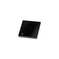
PIC18F43K20-E/MV Microchip Technology, PIC18F43K20-E/MV Datasheet - Page 266

PIC18F43K20-E/MV
Manufacturer Part Number
PIC18F43K20-E/MV
Description
8KB, Flash, 768bytes-RAM, 36I/O, 8-bit Family,nanowatt XLP 40 UQFN 5x5x0.5mm TUB
Manufacturer
Microchip Technology
Series
PIC® XLP™ 18Fr
Datasheet
1.PIC18F25K20T-ISS.pdf
(456 pages)
Specifications of PIC18F43K20-E/MV
Processor Series
PIC18
Core
PIC18F
Data Bus Width
8 bit
Program Memory Type
Flash
Program Memory Size
8 KB
Data Ram Size
512 B
Interface Type
I2C, SPI, SCI, USB, MSSP, RJ11
Maximum Clock Frequency
64 MHz
Number Of Programmable I/os
35
Number Of Timers
4
Operating Supply Voltage
1.8 V to 3.6 V
Maximum Operating Temperature
+ 125 C
Mounting Style
SMD/SMT
Package / Case
UQFN-40
Development Tools By Supplier
MPLAB Integrated Development Environment
Minimum Operating Temperature
- 40 C
Operating Temperature Range
- 40 C to + 125 C
Supply Current (max)
30 uA
Core Processor
PIC
Core Size
8-Bit
Speed
48MHz
Connectivity
I²C, SPI, UART/USART
Peripherals
Brown-out Detect/Reset, HLVD, POR, PWM, WDT
Number Of I /o
35
Eeprom Size
256 x 8
Ram Size
512 x 8
Voltage - Supply (vcc/vdd)
1.8 V ~ 3.6 V
Data Converters
A/D 14x10b
Oscillator Type
Internal
Operating Temperature
-40°C ~ 125°C
Lead Free Status / Rohs Status
Details
- Current page: 266 of 456
- Download datasheet (4Mb)
PIC18F2XK20/4XK20
19.1
When configuring and using the ADC the following
functions must be considered:
• Port configuration
• Channel selection
• ADC voltage reference selection
• ADC conversion clock source
• Interrupt control
• Results formatting
19.1.1
The ANSEL, ANSELH, TRISA, TRISB and TRISE reg-
isters all configure the A/D port pins. Any port pin
needed as an analog input should have its correspond-
ing ANSx bit set to disable the digital input buffer and
TRISx bit set to disable the digital output driver. If the
TRISx bit is cleared, the digital output level (V
V
The A/D operation is independent of the state of the
ANSx bits and the TRIS bits.
19.1.2
The CHS bits of the ADCON0 register determine which
channel is connected to the sample and hold circuit.
When changing channels, a delay is required before
starting the next conversion. Refer to Section 19.2
“ADC Operation” for more information.
19.1.3
The VCFG bits of the ADCON1 register provide
independent control of the positive and negative
voltage references. The positive voltage reference can
be either V
the negative voltage reference can be either V
external voltage source.
DS41303G-page 266
OL
Note 1: When reading the PORT register, all pins
) will be converted.
2: Analog levels on any pin with the corre-
3: The
ADC Configuration
DD
PORT CONFIGURATION
CHANNEL SELECTION
ADC V
with their corresponding ANSx bit set
read as cleared (a low level). However,
analog conversion of pins configured as
digital inputs (ANSx bit cleared and
TRISx
converted.
sponding ANSx bit cleared may cause the
digital input buffer to consume current out
of the device’s specification limits.
Register 3H configures PORTB pins to
reset as analog or digital pins by
controlling how the bits in ANSELH are
reset.
or an external voltage source. Likewise,
PBADEN
OLTAGE REFERENCE
bit
set)
bit
will
in
be
Configuration
accurately
SS
OH
or an
or
19.1.4
The ADCON2 register allows the user to select an
acquisition time that occurs each time the GO/DONE
bit is set.
Acquisition time is set with the ACQT<2:0> bits of the
ADCON2 register. Acquisition delays cover a range of
2 to 20 T
module continues to sample the input for the selected
acquisition time, then automatically begins a conver-
sion. Since the acquisition time is programmed, there is
no need to wait for an acquisition time between select-
ing a channel and setting the GO/DONE bit.
Manual
ACQT<2:0> = 000. When the GO/DONE bit is set,
sampling is stopped and a conversion begins. The user
is responsible for ensuring the required acquisition time
has passed between selecting the desired input
channel and setting the GO/DONE bit. This option is
also the default Reset state of the ACQT<2:0> bits and
is compatible with devices that do not offer
programmable acquisition times.
In either case, when the conversion is completed, the
GO/DONE bit is cleared, the ADIF flag is set and the
A/D begins sampling the currently selected channel
again. When an acquisition time is programmed, there
is no indication of when the acquisition time ends and
the conversion begins.
19.1.5
The source of the conversion clock is software select-
able via the ADCS bits of the ADCON2 register. There
are seven possible clock options:
• F
• F
• F
• F
• F
• F
• F
The time to complete one bit conversion is defined as
T
as shown in Figure 19-3.
For correct conversion, the appropriate T
must be met. See A/D conversion requirements in
Table 26-25 for more information. Table 19-1 gives
examples of appropriate ADC clock selections.
AD
Note:
OSC
OSC
OSC
OSC
OSC
OSC
RC
. One full 10-bit conversion requires 11 T
(dedicated internal oscillator)
/2
/4
/8
/16
/32
/64
AD
SELECTING AND CONFIGURING
ACQUISITION TIME
. When the GO/DONE bit is set, the A/D
Unless using the F
system clock frequency will change the
ADC
adversely affect the ADC result.
acquisition
CONVERSION CLOCK
clock
2010 Microchip Technology Inc.
frequency,
is
RC
, any changes in the
selected
AD
which
specification
AD
periods
when
may
Related parts for PIC18F43K20-E/MV
Image
Part Number
Description
Manufacturer
Datasheet
Request
R

Part Number:
Description:
Manufacturer:
Microchip Technology Inc.
Datasheet:

Part Number:
Description:
Manufacturer:
Microchip Technology Inc.
Datasheet:

Part Number:
Description:
Manufacturer:
Microchip Technology Inc.
Datasheet:

Part Number:
Description:
Manufacturer:
Microchip Technology Inc.
Datasheet:

Part Number:
Description:
Manufacturer:
Microchip Technology Inc.
Datasheet:

Part Number:
Description:
Manufacturer:
Microchip Technology Inc.
Datasheet:

Part Number:
Description:
Manufacturer:
Microchip Technology Inc.
Datasheet:

Part Number:
Description:
Manufacturer:
Microchip Technology Inc.
Datasheet:


