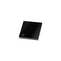
PIC18F43K20-E/MV Microchip Technology, PIC18F43K20-E/MV Datasheet - Page 28

PIC18F43K20-E/MV
Manufacturer Part Number
PIC18F43K20-E/MV
Description
8KB, Flash, 768bytes-RAM, 36I/O, 8-bit Family,nanowatt XLP 40 UQFN 5x5x0.5mm TUB
Manufacturer
Microchip Technology
Series
PIC® XLP™ 18Fr
Datasheet
1.PIC18F25K20T-ISS.pdf
(456 pages)
Specifications of PIC18F43K20-E/MV
Processor Series
PIC18
Core
PIC18F
Data Bus Width
8 bit
Program Memory Type
Flash
Program Memory Size
8 KB
Data Ram Size
512 B
Interface Type
I2C, SPI, SCI, USB, MSSP, RJ11
Maximum Clock Frequency
64 MHz
Number Of Programmable I/os
35
Number Of Timers
4
Operating Supply Voltage
1.8 V to 3.6 V
Maximum Operating Temperature
+ 125 C
Mounting Style
SMD/SMT
Package / Case
UQFN-40
Development Tools By Supplier
MPLAB Integrated Development Environment
Minimum Operating Temperature
- 40 C
Operating Temperature Range
- 40 C to + 125 C
Supply Current (max)
30 uA
Core Processor
PIC
Core Size
8-Bit
Speed
48MHz
Connectivity
I²C, SPI, UART/USART
Peripherals
Brown-out Detect/Reset, HLVD, POR, PWM, WDT
Number Of I /o
35
Eeprom Size
256 x 8
Ram Size
512 x 8
Voltage - Supply (vcc/vdd)
1.8 V ~ 3.6 V
Data Converters
A/D 14x10b
Oscillator Type
Internal
Operating Temperature
-40°C ~ 125°C
Lead Free Status / Rohs Status
Details
- Current page: 28 of 456
- Download datasheet (4Mb)
PIC18F2XK20/4XK20
2.2
The OSCCON register (Register 2-1) controls several
aspects of the device clock’s operation, both in full
power operation and in power-managed modes.
• Main System Clock Selection (SCS)
• Internal Frequency selection bits (IRCF)
• Clock Status bits (OSTS, IOFS)
• Power management selection (IDLEN)
2.2.1
The System Clock Select bits, SCS<1:0>, select the
main clock source. The available clock sources are
• Primary clock defined by the FOSC<3:0> bits of
• Secondary clock (Timer1 oscillator)
• Internal oscillator block (HFINTOSC and
The clock source changes immediately after one or
more of the bits is written to, following a brief clock tran-
sition interval. The SCS bits are cleared to select the
primary clock on all forms of Reset.
2.2.2
The
(IRCF<2:0>) select the frequency output of the internal
oscillator block. The choices are the LFINTOSC source
(31 kHz), the HFINTOSC source (16 MHz) or one of
the frequencies derived from the HFINTOSC post-
scaler (31.25 kHz to 8 MHz). If the internal oscillator
block is supplying the main clock, changing the states
of these bits will have an immediate change on the
internal oscillator’s output. On device Resets, the out-
put frequency of the internal oscillator is set to the
default frequency of 1 MHz.
2.2.3
When a nominal output frequency of 31 kHz is selected
(IRCF<2:0> = 000), users may choose which internal
oscillator acts as the source. This is done with the
INTSRC bit of the OSCTUNE register. Setting this bit
selects the HFINTOSC as a 31.25 kHz clock source by
enabling the divide-by-512 output of the HFINTOSC
postscaler. Clearing INTSRC selects LFINTOSC (nom-
inally 31 kHz) as the clock source.
This option allows users to select the tunable and more
precise HFINTOSC as a clock source, while maintain-
ing power savings with a very low clock speed. Regard-
less of the setting of INTSRC, LFINTOSC always
remains the clock source for features such as the
Watchdog Timer and the Fail-Safe Clock Monitor.
DS41303G-page 28
CONFIG1H. The primary clock can be the primary
oscillator, an external clock, or the internal oscilla-
tor block.
LFINTOSC).
Internal
Oscillator Control
MAIN SYSTEM CLOCK SELECTION
INTERNAL FREQUENCY
SELECTION
LOW FREQUENCY SELECTION
Oscillator
Frequency
Select
bits
2.2.4
The OSTS and IOFS bits of the OSCCON register, and
the T1RUN bit of the T1CON register, indicate which
clock source is currently providing the main clock. The
OSTS bit indicates that the Oscillator Start-up Timer
has timed out and the primary clock is providing the
device clock. The IOFS bit indicates when the internal
oscillator block has stabilized and is providing the
device clock in HFINTOSC Clock modes. The IOFS
and OSTS Status bits will both be set when
SCS<1:0> = 00 and HFINTOSC is the primary clock.
The T1RUN bit indicates when the Timer1 oscillator is
providing the device clock in secondary clock modes.
When SCS<1:0> 00, only one of these three bits will
be set at any time. If none of these bits are set, the
LFINTOSC is providing the clock or the HFINTOSC
has just started and is not yet stable.
2.2.5
The IDLEN bit of the OSCCON register determines if
the device goes into Sleep mode or one of the Idle
modes when the SLEEP instruction is executed.
The use of the flag and control bits in the OSCCON
register is discussed in more detail in Section 3.0
“Power-Managed Modes”.
Note 1: The Timer1 oscillator must be enabled to
2: It is recommended that the Timer1
CLOCK STATUS
POWER MANAGEMENT
select the secondary clock source. The
Timer1 oscillator is enabled by setting the
T1OSCEN bit of the T1CON register. If
the Timer1 oscillator is not enabled, then
the main oscillator will continue to run
from the previously selected source. The
source will then switch to the secondary
oscillator after the T1OSCEN bit is set.
oscillator be operating and stable before
selecting the secondary clock source or a
very long delay may occur while the
Timer1 oscillator starts.
2010 Microchip Technology Inc.
Related parts for PIC18F43K20-E/MV
Image
Part Number
Description
Manufacturer
Datasheet
Request
R

Part Number:
Description:
Manufacturer:
Microchip Technology Inc.
Datasheet:

Part Number:
Description:
Manufacturer:
Microchip Technology Inc.
Datasheet:

Part Number:
Description:
Manufacturer:
Microchip Technology Inc.
Datasheet:

Part Number:
Description:
Manufacturer:
Microchip Technology Inc.
Datasheet:

Part Number:
Description:
Manufacturer:
Microchip Technology Inc.
Datasheet:

Part Number:
Description:
Manufacturer:
Microchip Technology Inc.
Datasheet:

Part Number:
Description:
Manufacturer:
Microchip Technology Inc.
Datasheet:

Part Number:
Description:
Manufacturer:
Microchip Technology Inc.
Datasheet:


