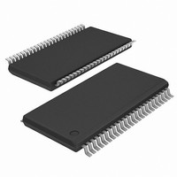
ICS951402AGLF IDT, Integrated Device Technology Inc, ICS951402AGLF Datasheet

ICS951402AGLF
Specifications of ICS951402AGLF
Available stocks
Related parts for ICS951402AGLF
ICS951402AGLF Summary of contents
Page 1
Integrated Circuit Systems, Inc. Programmable Timing Control Hub™ for P4™ processor Recommended Application: ATI chipset, P4 system, Banias system Output Features: • Pairs of differential CPUCLKs (differential current mode) • SDRAM @ 3.3V • ...
Page 2
Integrated Circuit Systems, Inc. Pin Description PIN NUMBER PIN NAME 1 VDDREF 2 FS0/REF0 3 FS1/REF1 4 FS2/REF2 5 GNDREF GND 9 VDD 10 *VttPWR_GD/PD# 11 PCI66/33#_SEL 12 PCI_STOP#* 13 VDDPCI 14 FS3/PCICLK_F0 15 FS4/PCICLK_F1 ...
Page 3
Integrated Circuit Systems, Inc. Table 1: Clock Power Management Truth Table Byte 6 Byte 6 CPU_ PD# Bit 6 Bit 7 STOP ...
Page 4
Integrated Circuit Systems, Inc. 2 General I C serial interface information for the ICS951402 How to Write: • Controller (host) sends a start bit. • Controller (host) sends the write address D2 • ICS clock will acknowledge • Controller (host) ...
Page 5
Integrated Circuit Systems, Inc. Serial Configuration Command Bitmap CPU MHz FS4 FS3 FS2 FS1 FS0 100. 133. 200. 166.65 0 ...
Page 6
Integrated Circuit Systems, Inc Table: Reserved Register Byte 0 Pin # Name - Reserved Bit 7 - Reserved Bit 6 Bit 5 - Reserved - Reserved Bit 4 Bit 3 - Reserved - Reserved Bit 2 - ...
Page 7
Integrated Circuit Systems, Inc Table: Reserved Register Byte 3 Pin # Name - Reserved Bit 7 - Reserved Bit 6 - Reserved Bit 5 - Reserved Bit 4 - Reserved Bit 3 Bit 2 - Reserved Bit ...
Page 8
Integrated Circuit Systems, Inc Table: Output Control Register Byte 6 Pin # Name - CPU_STOP# Bit 7 - PD# Bit 6 Bit 5 - PCI_F0 - PCI_F1 Bit 4 Bit 3 - CPUT/C_0 Bit 2 - CPUT/C_1 ...
Page 9
Integrated Circuit Systems, Inc Table: Watchdog Timer Register Byte 9 Pin # Name - WD7 Bit 7 Bit 6 - WD6 - WD5 Bit 5 Bit 4 - WD4 - WD3 Bit 3 Bit 2 - WD2 ...
Page 10
Integrated Circuit Systems, Inc Table: VCO Frequency Control Register Byte 12 Pin # Name - N Div7 Bit Div6 Bit Div5 Bit Div4 Bit Div3 ...
Page 11
Integrated Circuit Systems, Inc Table: Output Divider Control Register Byte 15 Pin # Name - SD Div3 Bit Div2 Bit 6 Bit Div1 Bit Div0 Bit 3 - ...
Page 12
Integrated Circuit Systems, Inc Table: Output Divider Control Register Byte 16 Pin # Name Bit 7 - AGP Div3 Bit 6 - AGP Div2 Bit 5 - AGP Div1 - AGP Div0 Bit 4 Bit 3 - ...
Page 13
Integrated Circuit Systems, Inc. Table 4:Skew Specification on Output Mode Bit3 Bit2 Table: Group Skew Control Register Byte 19 Pin # Name - Reserved Bit 7 - Reserved Bit ...
Page 14
Integrated Circuit Systems, Inc Table: Slew Rate Control Register Byte 21 Pin # Name Bit 7 - 24_48Slw1 - 24_48Slw0 Bit 6 Bit 5 - AGPSlw1 - AGPSlw0 Bit 4 Bit 3 - Reserved - Reserved Bit ...
Page 15
Integrated Circuit Systems, Inc Table: Reserved Control Register Byte 24 Pin # Name - Reserved Bit 7 - Reserved Bit 6 - Reserved Bit 5 - Reserved Bit 4 - Reserved Bit 3 - Reserved Bit 2 ...
Page 16
Integrated Circuit Systems, Inc. Absolute Maximum Ratings Core Supply Voltage . . . . . . . . . . . . . . . . . . . . . . 4.6 V I/O Supply Voltage . . . ...
Page 17
Integrated Circuit Systems, Inc. Electrical Characteristics - CPU (0.7V Select 70C; VDD=3.3V +/-5 PARAMETER SYMBOL Current Source Output Impedance Output High Voltage Output Low Voltage Voltage High VHigh Voltage Low Max Voltage Min Voltage ...
Page 18
Integrated Circuit Systems, Inc. Electrical Characteristics - VCH, 48MHz DOT, 48MHz, USB 70C; VDD=3.3V +/-5 PARAMETER SYMBOL Output Frequency Output Impedance R Output High Voltage V Output Low Voltage V Output High Current Output ...
Page 19
Integrated Circuit Systems, Inc. Electrical Characteristics - REF 70C; VDD=3.3V +/-5 PARAMETER SYMBOL Output Frequency Output Impedance R Output High Voltage V Output Low Voltage V Output High Current Output Low Current Rise Time ...
Page 20
Integrated Circuit Systems, Inc. Shared Pin Operation - Input/Output Pins The I/O pins designated by (input/output) serve as dual signal functions to the device. During initial power-up, they act as input pins. The logic level (voltage) that is present on ...
Page 21
Integrated Circuit Systems, Inc. PCI_STOP# - Assertion (transition from logic "1" to logic "0") The impact of asserting the PCI_STOP# signal will be the following. All PCI and stoppable PCI_F clocks will latch low in their next high to low ...
Page 22
Integrated Circuit Systems, Inc INDEX INDEX AREA AREA Ordering Information ICS951402yGLF-T Example: ICS XXXX y G LF- T 0660—05/05/05 c SYMBOL ...
Page 23
Integrated Circuit Systems, Inc INDEX INDEX AREA AREA 45° .10 (.004) C .10 (.004) C Ordering Information ICS951402yFLF-T Example: ICS XXXX y F LF- T Designation for tape ...


