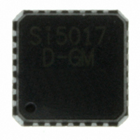
SI5017-D-GM Silicon Laboratories Inc, SI5017-D-GM Datasheet - Page 20

SI5017-D-GM
Manufacturer Part Number
SI5017-D-GM
Description
IC CLOCK/DATA RECOVERY 28MLP
Manufacturer
Silicon Laboratories Inc
Type
Clock and Data Recovery (CDR)r
Datasheet
1.SI5017-D-GM.pdf
(26 pages)
Specifications of SI5017-D-GM
Input
Differential
Output
CML
Frequency - Max
2.7GHz
Voltage - Supply
3.135 V ~ 3.465 V
Operating Temperature
-40°C ~ 85°C
Mounting Type
Surface Mount
Package / Case
28-VQFN Exposed Pad, 28-HVQFN, 28-SQFN, 28-DHVQFN
Frequency-max
2.7GHz
Lead Free Status / RoHS Status
Contains lead / RoHS non-compliant
Other names
336-1279
Si5017
20
Pin #
10
12
13
15
16
17
19
20
7
8
9
RESET/CAL
Pin Name
DSQLCH
DOUT+
DOUT–
REXT
DIN+
DIN–
GND
LOS
LOL
LTR
Table 8. Si5017 Pin Descriptions (Continued)
I/O
O
O
O
I
I
I
Signal Level
See Table 2
LVTTL
LVTTL
LVTTL
LVTTL
LVTTL
GND
CML
Rev. 1.5
Loss-of-Lock.
This output is driven low when the recovered clock
frequency deviates from the reference clock by the
amount specified in Table 4 on page 9. If no exter-
nal reference is supplied, this signal will be active
when the internal PLL is no longer locked to the
incoming data.
Lock-to-Reference.
When this pin is low, the DSPLL disregards the data
inputs. If an external reference is supplied, the out-
put clock locks to the supplied reference. If no
external reference is used, the DSPLL locks the
control loop until LTR is released.
Note: This input has a weak internal pullup.
Loss-of-Signal.
This output pin is driven low when the input signal is
below the threshold set via LOS_LVL. (LOS opera-
tion is guaranteed only when ac coupling is used on
the DIN inputs.)
Data Squelch.
When driven high, this pin forces the data present
on DOUT+ to zero and DOUT– to one. For normal
operation, this pin should be low. DSQLCH may be
used during LOS/LOL conditions to prevent random
data from being presented to the system.
Note: This input has a weak internal pulldown.
Differential Data Input.
Clock and data are recovered from the differential
signal present on these pins. AC coupling is
recommended.
Production Test Input.
This pin is used during production testing and must
be tied to GND for normal operation.
Differential Data Output.
The data output signal is a retimed version of the
data recovered from the signal present on DIN.
Reset/Calibrate.
Driving this input high for at least 1 µs will reset
internal device circuitry. A high to low transition on
this pin will force a DSPLL calibration. For normal
operation, drive this pin low.
Note: This input has a weak internal pulldown.
External Bias Resistor.
This resistor is used to establish internal bias cur-
rents within the device. This pin must be connected
to GND through a 10 k1resistor.
Description


