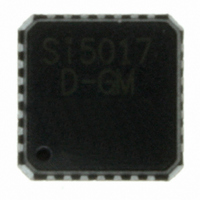
SI5017-D-GM Silicon Laboratories Inc, SI5017-D-GM Datasheet - Page 21

SI5017-D-GM
Manufacturer Part Number
SI5017-D-GM
Description
IC CLOCK/DATA RECOVERY 28MLP
Manufacturer
Silicon Laboratories Inc
Type
Clock and Data Recovery (CDR)r
Datasheet
1.SI5017-D-GM.pdf
(26 pages)
Specifications of SI5017-D-GM
Input
Differential
Output
CML
Frequency - Max
2.7GHz
Voltage - Supply
3.135 V ~ 3.465 V
Operating Temperature
-40°C ~ 85°C
Mounting Type
Surface Mount
Package / Case
28-VQFN Exposed Pad, 28-HVQFN, 28-SQFN, 28-DHVQFN
Frequency-max
2.7GHz
Lead Free Status / RoHS Status
Contains lead / RoHS non-compliant
Other names
336-1279
GND Pad
Pin #
22
23
24
26
27
28
CLKOUT–
CLKOUT+
CLKDSBL
BER_ALM
Pin Name
BER_LVL
GND
NC
Table 8. Si5017 Pin Descriptions (Continued)
I/O
O
O
I
I
Signal Level
LVTTL
LVTTL
GND
CML
Rev. 1.5
Differential Clock Output.
The output clock is recovered from the data signal
present on DIN except when LTR is asserted or the
LOL state has been entered.
Clock Disable.
When this input is high, the CLKOUT output drivers
are disabled. For normal operation, this pin should
be low.
Note: This input has a weak internal pulldown.
Bit Error Rate Level Control.
The BER threshold level is set by applying a volt-
age to this pin. When the BER exceeds the pro-
grammed threshold, BER_ALM is driven low. If this
pin is tied to GND, BER_ALM is disabled.
Bit Error Rate Alarm.
This pin will be driven low to indicate that the BER
threshold set by BER_LVL has been exceeded.
There is no hysteresis.
No Connect.
Leave this pin disconnected.
Supply Ground.
Nominally 0.0 V. The GND pad found on the bottom
of the 28-lead QFN (see Figure 16 on page 23)
must be connected directly to supply ground.
Minimize the ground path inductance for optimal
performance.
Description
Si5017
21


