LMK04001BISQE/NOPB National Semiconductor, LMK04001BISQE/NOPB Datasheet - Page 22
LMK04001BISQE/NOPB
Manufacturer Part Number
LMK04001BISQE/NOPB
Description
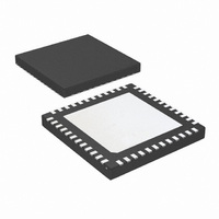
IC CLOCK COND 1.5GHZ W/PLL 48LLP
Manufacturer
National Semiconductor
Series
PowerWise®r
Type
Clock Conditionerr
Datasheet
1.LMK04010BISQENOPB.pdf
(54 pages)
Specifications of LMK04001BISQE/NOPB
Pll
Yes
Input
LVCMOS
Output
LVCMOS, 2VPECL, LVPECL
Number Of Circuits
1
Ratio - Input:output
2:7
Differential - Input:output
Yes/Yes
Frequency - Max
1.57GHz
Divider/multiplier
Yes/Yes
Voltage - Supply
3.15 V ~ 3.45 V
Operating Temperature
-40°C ~ 85°C
Mounting Type
Surface Mount
Package / Case
48-LLP
Frequency-max
1.57GHz
Lead Free Status / RoHS Status
Lead free / RoHS Compliant
Other names
LMK04001BISQETR
Available stocks
Company
Part Number
Manufacturer
Quantity
Price
Company:

Part Number:
LMK04001BISQE/NOPB
Manufacturer:
NS
Quantity:
250


www.national.com
11.0 Serial Data Timing Diagram
Register programming information on the DATAuWire pin is clocked into a shift register on each rising edge of the CLKuWire signal.
On the rising edge of the LEuWire signal, the register is sent from the shift register to the register addressed. A slew rate of at least
30 V/µs is recommended for these signals. After programming is complete the CLKuWire, DATAuWire, and LEuWire signals should
be returned to a low state. If the CLKuWire or DATAuWire lines are toggled while the VCO is in lock, as is sometimes the case
when these lines are shared with other parts, the phase noise may be degraded during this programming.
12.0 Charge Pump Current Specification Definitions
I1 = Charge Pump Sink Current at V
I2 = Charge Pump Sink Current at V
I3 = Charge Pump Sink Current at V
I4 = Charge Pump Source Current at V
I5 = Charge Pump Source Current at V
I6 = Charge Pump Source Current at V
CPout
CPout
CPout
CPout
CPout
CPout
= V
= V
= ΔV
= V
= V
= ΔV
CC
CC
/2
CC
CC
- ΔV
/2
- ΔV
22
30027131
30027103
Related parts for LMK04001BISQE/NOPB
Image
Part Number
Description
Manufacturer
Datasheet
Request
R

Part Number:
Description:
National Semiconductor [8-Bit D/A Converter]
Manufacturer:
National Semiconductor
Datasheet:
Part Number:
Description:
National Semiconductor [Media Coprocessor]
Manufacturer:
National Semiconductor
Datasheet:
Part Number:
Description:
Digitally Controlled Tone and Volume Circuit with Stereo Audio Power Amplifier, Microphone Preamp Stage and National 3D Sound
Manufacturer:
National Semiconductor
Datasheet:
Part Number:
Description:
Digitally Controlled Tone and Volume Circuit with Stereo Audio Power Amplifier, Microphone Preamp Stage and National 3D Sound
Manufacturer:
National Semiconductor
Datasheet:
Part Number:
Description:
AC97 Rev 2 Codec with Sample Rate Conversion and National 3D Sound
Manufacturer:
National Semiconductor
Part Number:
Description:
Manufacturer:
National Semiconductor
Datasheet:
Part Number:
Description:
Manufacturer:
National Semiconductor
Datasheet:
Part Number:
Description:
General Purpose, Low Voltage, Low Power, Rail-to-Rail Output Operational Amplifiers
Manufacturer:
National Semiconductor
Datasheet:
Part Number:
Description:
8-bit 20 MSPS flash A/D converter.
Manufacturer:
National Semiconductor
Datasheet:
Part Number:
Description:
Low Noise Quad Operational Amplifier
Manufacturer:
National Semiconductor
Datasheet:
Part Number:
Description:
Quad Differential Line Receivers
Manufacturer:
National Semiconductor
Datasheet:
Part Number:
Description:
Quad High Speed Trapezoidal? Bus Transceiver
Manufacturer:
National Semiconductor
Datasheet:
Part Number:
Description:
Dual Line Receiver
Manufacturer:
National Semiconductor
Datasheet:
Part Number:
Description:
TTL to 10k ECL Level Translator with Latch
Manufacturer:
National Semiconductor
Datasheet: