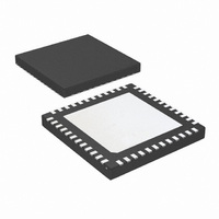
LMK04001BISQE/NOPB National Semiconductor, LMK04001BISQE/NOPB Datasheet - Page 50

LMK04001BISQE/NOPB
Manufacturer Part Number
LMK04001BISQE/NOPB
Description
IC CLOCK COND 1.5GHZ W/PLL 48LLP
Manufacturer
National Semiconductor
Series
PowerWise®r
Type
Clock Conditionerr
Datasheet
1.LMK04010BISQENOPB.pdf
(54 pages)
Specifications of LMK04001BISQE/NOPB
Pll
Yes
Input
LVCMOS
Output
LVCMOS, 2VPECL, LVPECL
Number Of Circuits
1
Ratio - Input:output
2:7
Differential - Input:output
Yes/Yes
Frequency - Max
1.57GHz
Divider/multiplier
Yes/Yes
Voltage - Supply
3.15 V ~ 3.45 V
Operating Temperature
-40°C ~ 85°C
Mounting Type
Surface Mount
Package / Case
48-LLP
Frequency-max
1.57GHz
Lead Free Status / RoHS Status
Lead free / RoHS Compliant
Other names
LMK04001BISQETR
Available stocks
Company
Part Number
Manufacturer
Quantity
Price
Company:
Part Number:
LMK04001BISQE/NOPB
Manufacturer:
NS
Quantity:
250
www.national.com
Figure 22 compares the phase noise of two different VCXOs:
VCXO “A” and VCXO “B”. Both VCXOs have a center fre-
quency of 100 MHz. The figure of merit, RMS jitter, is mea-
This plot shows that VCXO “B” exhibits superior phase noise
when compared to VCXO “A”. Both VCXOs offer excellent
jitter performance from 100 Hz to 200 kHz. VCXO “A” exhibits
RMS jitter of 151 femtoseconds (fs), while VCXO “B” has RMS
jitter of 90 fs.
Figures 23, 24, 25 present a side-by-side comparison of clock
output phase noise at 250 MHz, organized by output format
and associated VCXO. The total RMS jitter listed on the plots
is integrated from 100 Hz to 20 MHz. Examining these plots,
the clock output phase noise associated with VCXO “B” is
superior in all cases. The average improvement in RMS jitter
due to VCXO “B” is approximately 47 fs. The plots show the
primary difference in clock output phase noise is in the band
from 100 Hz to approximately 4 kHz. Across this range, the
VCXO phase noise dominates that of the PLL, given the loop
bandwidth of this design, which is 152 kHz. Above 4 kHz, the
PLL noise dominates (inside the loop bandwidth), so it is ba-
FIGURE 22. VCXO Phase Noise Comparison, 100 MHz
50
sured over the bandwidth 100 Hz to 200 kHz. This is the most
relevant integration bandwidth for the VCXO because it will
have the most impact inside the loop bandwidth of PLL2.
sically the same for either VCXO. Comparing the jitter of two
VCXOs in the 100 Hz to 4 kHz band, it can be shown that
VCXO “A” exhibits jitter of 142 fs, and VCXO “B” exhibits jitter
of 90 fs. The difference, 52 fs, accounts for the majority of the
average difference in RMS jitter at the clock outputs when
comparing VCXOs.
The PLL configurations listed below were the same for both
VCXOs/LMK040xx pair:
•
•
•
•
PLL1 loop filter components: C1 = 100 nF, C2 = 680 nF,
R2 = 39 kΩ
PLL1 f
PLL2 loop filter components: C1 = 0, C2 = 12 nF, R2 = 1.8
kΩ
PLL2 f
kHz
PD
PD
= 1 MHz, CP gain = 100 µA, loop BW = 20 Hz
= 25 MHz, CP gain = 3200 µA, loop BW = 152
30027147


