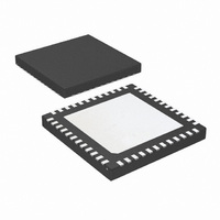
LMK04001BISQE/NOPB National Semiconductor, LMK04001BISQE/NOPB Datasheet - Page 38

LMK04001BISQE/NOPB
Manufacturer Part Number
LMK04001BISQE/NOPB
Description
IC CLOCK COND 1.5GHZ W/PLL 48LLP
Manufacturer
National Semiconductor
Series
PowerWise®r
Type
Clock Conditionerr
Datasheet
1.LMK04010BISQENOPB.pdf
(54 pages)
Specifications of LMK04001BISQE/NOPB
Pll
Yes
Input
LVCMOS
Output
LVCMOS, 2VPECL, LVPECL
Number Of Circuits
1
Ratio - Input:output
2:7
Differential - Input:output
Yes/Yes
Frequency - Max
1.57GHz
Divider/multiplier
Yes/Yes
Voltage - Supply
3.15 V ~ 3.45 V
Operating Temperature
-40°C ~ 85°C
Mounting Type
Surface Mount
Package / Case
48-LLP
Frequency-max
1.57GHz
Lead Free Status / RoHS Status
Lead free / RoHS Compliant
Other names
LMK04001BISQETR
Available stocks
Company
Part Number
Manufacturer
Quantity
Price
Company:
Part Number:
LMK04001BISQE/NOPB
Manufacturer:
NS
Quantity:
250
www.national.com
16.12 REGISTER 15
16.12.1 PLL2_N: PLL2_N Counter
The PLL2_N Counter is 18 bits wide. It divides the output of
the VCO Divider and is connected to the PLL2 Phase Detec-
tor. Each time the PLL2_N Counter value is updated via the
uWire interface, an internal algorithm is triggered that opti-
mizes the VCO performance.
b4 b3 b2 b1 b0
0
0
0
0
0
0
0
0
0
0
0
0
0
0
0
0
1
1
1
1
1
1
1
1
1
1
1
1
1
1
1
1
PLL_MUX [4:0]
TABLE 27. PLL_MUX: LD Pin Selectable Outputs
0
0
0
0
0
0
0
0
1
1
1
1
1
1
1
1
0
0
0
0
0
0
0
0
1
1
1
1
1
1
1
1
0
0
0
0
1
1
1
1
0
0
0
0
1
1
1
1
0
0
0
0
1
1
1
1
0
0
0
0
1
1
1
1
0
0
1
1
0
0
1
1
0
0
1
1
0
0
1
1
0
0
1
1
0
0
1
1
0
0
1
1
0
0
1
1
0
1
0
1
0
1
0 PLL2 Analog Lock Detect Open Drain
1 PLL2 Analog Lock Detect Open Drain
0
1
0
1
0
1
0 PLL1 Digital Lock Detect Active HIGH
1
0
1
0
1
0
1
0
1
0
1
0
1
0
1
0
1
PLL1 Digital Lock Detect Active LOW
PLL2 Digital Lock Detect Active High
Inverted PLL1 and PLL2 Digital Lock
PLL2 Digital Lock Detect Active Low
PLL2 Analog Lock Detect Push Pull
PLL1 and PLL2 Digital Lock Detect
PLL2_N Divider Output / 2
PLL2_R Divider Output / 2
PLL1_N Divider Output / 2
PLL1_R Divider Output / 2
LD Output
Logic High
Logic Low
Reserved
Reserved
Reserved
Reserved
Reserved
Reserved
Reserved
Reserved
Reserved
Reserved
Reserved
Reserved
Reserved
Reserved
Reserved
Reserved
NMOS
PMOS
Detect
HiZ
38
16.12.2 PLL2_CP_GAIN: PLL2 Charge Pump Current and
Output Control
The PLL2 charge pump output current level is controlled with
the PLL2_CP_GAIN register. The following table presents the
charge pump current control values.
16.12.3 VCO_DIV: PLL2 VCO Divide Register
A divider is provided on the output of the PLL2 VCO to enable
a wide range of output clock frequencies. The output of this
divider is placed on the input path for the clock distribution
section, which feeds each of the individual clock channels.
The divider provides integer divide ratios from 2 to 8.
TABLE 29. PLL2_CP_GAIN: PLL2 Charge Pump Current
b17 b16
0
0
0
1
PLL2_CP_GAIN [1:0]
b3
TABLE 30. VCO_DIV: PLL2 VCO Divider Values
0
0
0
0
0
0
0
0
1
b1
TABLE 28. PLL2_N: PLL2_N Counter Values
X
0
0
1
1
0
0
0
1
...
...
VCO_DIV [3:0]
b2
0
0
0
0
1
1
1
1
0
b6 b5 b4 b3 b2 b1 b0
0
0
0
1
.
N [17:0]
b0
X
0
1
0
1
0
0
0
1
.
Selections
0
0
0
1
.
b1
0
0
1
1
0
0
1
1
0
0
0
0
1
.
CP_TRI
0
0
0
1
.
1
0
0
0
0
0
0
1
1
b0
.
0
1
0
1
0
1
0
1
0
0
1
0
1
.
Current (µA)
Charge
Pump
Not Valid
1600
3200
Hi-Z
VALUE
262143
100
400
Divide
Invalid
Invalid
Value
...
2
3
4
5
6
7
8
1
2


