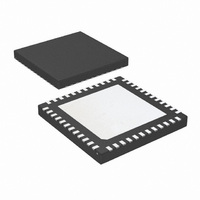
LMK04001BISQE/NOPB National Semiconductor, LMK04001BISQE/NOPB Datasheet - Page 44

LMK04001BISQE/NOPB
Manufacturer Part Number
LMK04001BISQE/NOPB
Description
IC CLOCK COND 1.5GHZ W/PLL 48LLP
Manufacturer
National Semiconductor
Series
PowerWise®r
Type
Clock Conditionerr
Datasheet
1.LMK04010BISQENOPB.pdf
(54 pages)
Specifications of LMK04001BISQE/NOPB
Pll
Yes
Input
LVCMOS
Output
LVCMOS, 2VPECL, LVPECL
Number Of Circuits
1
Ratio - Input:output
2:7
Differential - Input:output
Yes/Yes
Frequency - Max
1.57GHz
Divider/multiplier
Yes/Yes
Voltage - Supply
3.15 V ~ 3.45 V
Operating Temperature
-40°C ~ 85°C
Mounting Type
Surface Mount
Package / Case
48-LLP
Frequency-max
1.57GHz
Lead Free Status / RoHS Status
Lead free / RoHS Compliant
Other names
LMK04001BISQETR
Available stocks
Company
Part Number
Manufacturer
Quantity
Price
Company:
Part Number:
LMK04001BISQE/NOPB
Manufacturer:
NS
Quantity:
250
www.national.com
17.7 OPTIONAL CRYSTAL OSCILLATOR
IMPLEMENTATION (OSCin/OSCin*)
The LMK04000 family features supporting circuitry for a dis-
cretely implemented oscillator driving the OSCin port pins.
Figure 6 illustrates a reference design circuit for a crystal os-
cillator:
This circuit topology represents a parallel resonant mode os-
cillator design. When selecting a crystal for parallel reso-
nance, the total load capacitance, C
load capacitance is the sum of the tuning capacitance
(C
(C
and is given by:
C
Skyworks model SMV1249-074. A dual diode package with
common cathode and provides the variable capacitance for
tuning. The single diode capacitance ranges from approxi-
mately 31 pF at 0.3 V to 3.4 pF at 3 V. The capacitance range
of the dual package (anode to anode) is approximately 15.5
pF at 3 V to 1.7 pF at 0.3 V. The desired value of V
to the diode should be V
typical performance curve from the data sheet for the
SMV1249-074 indicates that the capacitance at this voltage
is approximately 6 pF (12 pF/2).
TUNE
TUNE
IN
), and stray capacitance due to PCB parasitics (C
), the capacitance seen looking into the OSCin port
is provided by the varactor diode shown in Figure 6,
CC
/2, or 1.65 V for V
FIGURE 6. Reference Design Circuit for Crystal Oscillator Option
L
, must be specified. The
30027164
CC
= 3.3 V. The
TUNE
applied
STRAY
),
44
The nominal input capacitance (C
OSCin pins is 6 pF. The stray capacitance (C
PCB should be minimized by arranging the oscillator circuit
layout to achieve trace lengths as short as possible and as
narrow as possible trace width (50 Ω characteristic
impedance is not required). As an example, assume that
C
Consequently the load capacitance specification for the crys-
tal in this case should be nominally 14 pF.
The 2.2 nF capacitors shown in the circuit are coupling ca-
pacitors that block the DC tuning voltage applied by the 4.7 k
and 10 k resistors. The value of these coupling capacitors
should be large, relative to the value of C
C
For a specific value of C
quency (F
F
C
S
STRAY
TUNE
1
= Series resonant frequency
= Motional capacitance of the crystal
), so that C
is 4 pF. The total load capacitance is nominally:
L
) of the parallel resonant mode circuit is:
TUNE
30027163
becomes the dominant capacitance.
L
, the corresponding resonant fre-
IN
) of the LMK04000 family
30027165
TUNE
(C
STRAY
C1
30027166
= C
) of the
C2
>>


