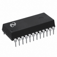
DP8572AN National Semiconductor, DP8572AN Datasheet - Page 4

DP8572AN
Manufacturer Part Number
DP8572AN
Description
IC REAL TIME CLOCK W/RAM 24 DIP
Manufacturer
National Semiconductor
Type
Clock/Calendar/NVSRAMr
Datasheet
1.DP8572AN.pdf
(22 pages)
Specifications of DP8572AN
Memory Size
44B
Time Format
HH:MM:SS:hh (12/24 hr)
Date Format
YY-MM-DD-dd
Interface
Parallel
Voltage - Supply
4.5 V ~ 5.5 V
Operating Temperature
-40°C ~ 85°C
Mounting Type
Through Hole
Package / Case
24-DIP (0.300", 7.62mm)
Lead Free Status / RoHS Status
Contains lead / RoHS non-compliant
Other names
*DP8572AN
DP8572
DP8572
Available stocks
Company
Part Number
Manufacturer
Quantity
Price
Part Number:
DP8572AN
Manufacturer:
TOSHIBA/东芝
Quantity:
20 000
Symbol
V
V
V
V
I
I
I
I
I
I
8572AM Military Version
Absolute Maximum Ratings
The 883 specifications are written to reflect the current
(at the time of printing) Rel Electrical Test Specifica-
tions (RETS) established by National Semiconductor for
this product For a copy of the latest version of the
RETS please contact your local National Semiconduc-
tor sales office or distributor
Supply Voltage (V
DC Input Voltage (V
DC Output Voltage (V
Storage Temperature Range
Power Dissipation (PD)
Lead Temperature (Soldering 10 sec )
DC Electrical Characteristics
V
Note 1 Absolute Maximum Ratings are those values beyond which damage to the device may occur
Note 2 Unless otherwise specified all voltages are referenced to ground
Note 3 For F
Note 4 This parameter (V
Note 5 This specification tests I
Note 6 This specification tests I
Note 7 OSC IN is driven by a signal generator Contents of the Test Register
IN
OZ
CC
CC
BB
BLK
IH
IL
OH
OL
CC
e
Single Supply Mode Data retention voltage is 2 2V min
In single Supply Mode (Power connected to V
5 0V
OSC
High Level Input Voltage
(Note 4)
Low Level Input Voltage
High Level Output Voltage
(Excluding OSC OUT)
Low Level Output Voltage
(Excluding OSC OUT)
Input Current (Except OSC IN)
Output TRI-STATE Current
Quiescent Supply Current
(Note 7)
Quiescent Supply Current
(Single Supply Mode)5 5V
(Note 7)
Standby Mode Battery
Supply Current
(Note 7)
Battery Leakage
g
e
10% V
4 194304 or 4 9152 MHz V
CC
IN
)
IH
OUT
)
Parameter
) is not tested on all pins at the same time
BB
)
CC
CC
e
with all power fail circuitry disabled by setting D7 of Interrupt Control Register 1 to 0
with all power fail circuitry enabled by setting D7 of Interrupt Control Register 1 to 1
3V
b
b
BB
0 5V to V
0 5V to V
b
minimum
CC
b
65 C to
0 5V to
pin) 4 5V
(Notes 1
5 5V
5 5V
5 5V
5 5V
5 5V
5 5V
5 5V
5 5V
5 5V
5 5V
5 5V
5 5V
5 5V
5 5V
5 5V
V
CC
CC
0V
0V
e
CC
a
500 mW
2 8V In battery backed mode V
a
a
a
s
150 C
260 C
7 0V
0 5V
0 5V
V
CC s
All Inputs Except OSC IN
OSC IN with External Clock
All Inputs Except OSC IN
OSC IN with External Clock
I
I
I
I
V
V
F
V
V
V
F
V
V
V
F
F
OSC OUT
Other Pins
F
F
2 2V
2)
OUT
OUT
OUT
OUT
IN
OUT
OSC
IN
IN
IN
OSC
IN
IN
BB
OSC
OSC
OSC
OSC
b
a
5 5V
e
e
e
e
e
e
25 C
55 C
125 C
e
e
4
e b
e b
e
e
s
e
e
e
e
e
e
e
V
V
V
V
V
V
00(H) and the MFO pin is not configured as buffered oscillator out
GND V
V
20 A
4 0 mA
CC
CC
CC
IH
CC
IH
V
32 768 kHz
4 9152 MHz
32 768 kHz
4 9152 MHz
32 768 kHz
4 9152 MHz
BB s
Operation Conditions
Supply Voltage (V
Supply Voltage (V
DC Input or Output Voltage
Operating Temperature (T
Electro-Static Discharge Rating
Typical Values
20 A
4 0 mA
Conditions
CC
e
or V
or V
e
or GND
or GND (Note 5)
or GND (Note 6)
or GND (Note 6)
(V
JA
Open Circuit
or GND
IN
GND
IL
IL
IN
4 0V
DIP
(Note 6)
(Note 6)
V
e
OUT
BB s
V
CC
)
Board
Socket
V
or GND
CC
CC
BB
b
) (Note 3)
) (Note 3)
0 4V
A
)
V
V
BB
CC
Min
b
b
b
2 0
3 5
b
b
5
5
5
0 1
0 1
b
Min
4 5
2 2 V
0 0
55
g
g
Max
0 25
12 0
275
400
0 8
0 1
0 1
1 0
7 5
1 5
3 5
3 5
20
40
10
8
CC
1 0
5 0
a
Max
V
5 5
125
1
b
CC
0 4
45 C W
52 C W
Units
Unit
mA
mA
mA
mA
mA
kV
V
V
V
V
V
V
V
V
V
V
V
C
A
A
A
A
A
A
A
A
A


