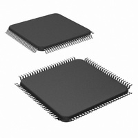
LM9833CCVJD/NOPB National Semiconductor, LM9833CCVJD/NOPB Datasheet - Page 13

LM9833CCVJD/NOPB
Manufacturer Part Number
LM9833CCVJD/NOPB
Description
IC USB IMAGE SCAN 48BIT 100-TOFP
Manufacturer
National Semiconductor
Datasheet
1.LM9833CCVJDNOPB.pdf
(42 pages)
Specifications of LM9833CCVJD/NOPB
Number Of Bits
16
Number Of Channels
3
Voltage - Supply, Analog
5V
Voltage - Supply, Digital
4.5 V ~ 5.5 V
Package / Case
100-TQFP, 100-VQFP
Lead Free Status / RoHS Status
Lead free / RoHS Compliant
Power (watts)
-
Other names
*LM9833CCVJD
*LM9833CCVJD/NOPB
LM9833CCVJD
*LM9833CCVJD/NOPB
LM9833CCVJD
Register Listing
Address
SENSOR CONTROL SETTINGS
INTEGRATION TIME ADJUST
STEPPER PHASE CORRECTION
0C
0D
0E
0F
10
12
13
14
15
16
17
18
19
1A
1B
11
Ø1 Polarity
Ø2 Polarity
RS Polarity
CP1 Polarity
CP2 Polarity
TR1 Polarity
TR2 Polarity
Ø1 Active/Off
Ø2 Active/Off
RS Active/Off
CP1 Active/Off
CP2 Active/Off
TR1 Active/Off
TR2 Active/Off
Number of TR Pulses
TR Pulse Duration
TR-Ø1 Guardband Duration
Optical Black Clamp Start
Optical Black Clamp End
Reset Pulse Start
Reset Pulse Stop
CP1 Pulse Start
CP1 Pulse Stop
CP2 Pulse Start
CP2 Pulse Stop
Reference Sample Position
Signal Sample Position
Integration Time Adjustment Function
TR to Stepper Phase Correction - MSB
TR to Stepper Phase Correction - LSB
(Continued)
Function
D
7
0
1
n n n n
n n n n n n n n
D
6
0
1
0
1
n n n n n n n t
D
0
1
0
1
n n n n n n
5
D
0
1
0
1
n n n n n
n n n n n
n n n n n
n n n n n
n n n n n
n n n n n
n n n n n
n n n n n
n n n n n
n n n n n
4
13
D
3
0
1
0
1
n n n n n+1 pixel periods (1-16)
D
0
1
0
1
2
D
0
1
0
1
1
D
0
0 Positive
1 Negative
0 Off
1 Active
Positive
Negative
Positive
Negative
Positive
Negative
Positive
Negative
Positive
Negative
Positive
Negative
Off
Active
Off
Active
Off
Active
Off
Active
Off
Active
Off
Active
1 TR Pulse
2 TR Pulses
n pixel periods (0-15)
pixel rate: n=0-23, line rate: n=0-7 MCLKs from Ø1 edge
pixel rate: n=0-23, line rate: n=0-7 MCLKs from Ø1 edge
pixel rate: n=0-23, line rate: n=0-7 MCLKs from Ø1 edge
pixel rate: n=0-23, line rate: n=0-7 MCLKs from Ø1 edge
pixel rate: n=0-23, line rate: n=0-7 MCLKs from Ø1 edge
pixel rate: n=0-23, line rate: n=0-7 MCLKs from Ø1 edge
pixel rate: n=0-23, line rate: n=0-7 MCLKs from Ø1 edge
pixel rate: n=0-23, line rate: n=0-7 MCLKs from Ø1 edge
pixel rate: n=0-23, line rate: n=0-7 MCLKs from Ø1 edge
pixel rate: n=0-23, line rate: n=0-7 MCLKs from Ø1 edge
First step of scan occurs n pixels (1 - 16383) after first
TR pulse. This register can be used to set the phase
between the TR pulses and the stepper motor pulses.
NOTE: a setting of n = 0 creates the maximum delay
(16384) pixels, which will increase scan time. If this
function is not used, this register should be set to 1.
READOUT
= n*t
INT
, n = 1 to 127. n=0 turns off function.
Value
www.national.com


