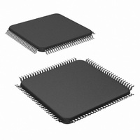
LM9833CCVJD/NOPB National Semiconductor, LM9833CCVJD/NOPB Datasheet - Page 38

LM9833CCVJD/NOPB
Manufacturer Part Number
LM9833CCVJD/NOPB
Description
IC USB IMAGE SCAN 48BIT 100-TOFP
Manufacturer
National Semiconductor
Datasheet
1.LM9833CCVJDNOPB.pdf
(42 pages)
Specifications of LM9833CCVJD/NOPB
Number Of Bits
16
Number Of Channels
3
Voltage - Supply, Analog
5V
Voltage - Supply, Digital
4.5 V ~ 5.5 V
Package / Case
100-TQFP, 100-VQFP
Lead Free Status / RoHS Status
Lead free / RoHS Compliant
Power (watts)
-
Other names
*LM9833CCVJD
*LM9833CCVJD/NOPB
LM9833CCVJD
*LM9833CCVJD/NOPB
LM9833CCVJD
Applications Information
14.0 QUESTIONS AND ANSWERS
Q Where is calibration done?
A Calibration is done on the host computer.
Q Does the LM9833 support 800dpi sensors? 400dpi? XXXdpi?
A Yes. The LM9833 will support any sensor up to a maximum of
15.0 GENERAL NOTES AND TROUBLESHOOTING TIPS
(mclk_divider)(HDPI_divider)(ITA) must be greater than or equal
to 6. If this condition is not met, the LM9833 will not work.
Make sure the gamma tables are programmed with a valid
gamma curve.
Make sure the multiplier gain coefficients are loaded and correct.
(Remember, a gain coefficient of 0 means a GAIN of x0, not x1. If
the gain coefficient = 0 the output code will always be 0.)
Remember that when the LM9833 is reset (reg08 = 0x20) or in
suspend for longer than a few milliseconds (consult your DRAM
datasheet), DRAM refresh will stop and the Gamma and Coeffi-
cient data may be corrupted.
Some of the CCD signals (RS, CP1, and CP2) can have a small
pulse when line_end occurs. Line_end resets these signals and
depending on how they are programmed to go on and off,
line_end can chop off the signal before its programmed off time.
This is not a problem because the truncation occurs at the end of
every line, after all the image data for that line has been digitized.
Registers 4 and 5 only autowrap to 0 from their highest possible
legal address. If an address higher than the highest legal address
is written, it will continue to increment from the illegal address, not
wrap to 0, and unknown operation may occur. This can not hap-
pen unless the host writes an illegal address to the dataport.
The absolute distance between reference sample and signal
sample must be 2 MCLKs or greater, whether CDS is on or off.
The range of values for the Optical Black (registers 0F and 10),
Reset Pulse (11 and 12), CP1 pulse (13 and 14), CP2 pulse (15
and 16), Reference Sample (17), and Signal Sample (18) settings
depend on the rate of the pixel data coming from the sensor.
Always make sure line length (data pixels end - data pixels start)
is >= the horizontal divider. For example, if you are dividing by 12,
the line length must be >=12.
The Line End (registers 20 and 21) setting must be programmed
as follows relative to the Data Pixels End (registers 24 and 25)
setting:
16383 pixels x 3 colors. Available horizontal resolutions are
calculated by the optical resolution of the scanner divided by
the HDPI_divider.
Pixel Rate Modes
Line Rate Modes
Mode
stepsize_ITA
Pixel Rate
MCLK/24
MCLK/8
=
stepsize
⋅
(Continued)
ITA+1
----------- -
Registers 0F to 18
ITA
Range
0 - 23
0 - 7
38
Line End must be >= Data Pixels End + 20
The Data Pixels Start (registers 22 and 23) setting must be >=the
Active Pixels Start (registers 1E and 1F) setting.
The correct Default Phase Difference (registers 51, 52, and 53)
must be set for a scan to restart properly following a pause in the
scanning. See the LM9833 software for information on setting the
DPD register.
The number of fullsteps skipped at the start of a scan may be one
less than the Fullsteps to Skip at Start of Scan (registers 4A and
4B) setting.
The Scanning Step Size (registers 46 and 47) and Fast Feed
Step Size (registers 48 and 49) settings must be > 2.
When reverse is enabled, the LM9833 always stops on Red (line
rate color). When reverse is disabled, it will stop on any color.
The contents of register 01 is not reset by the start of a new scan,
but it is updated to the correct value after the first line has been
scanned. To reset this counter prior to starting a scan, the chip
can be briefly reset (register 7 = 0x20). Since resetting the chip
may have undesired consequences (turning the lamp off briefly,
interrupting DRAM refresh), it is also acceptable to simply wait
until register 01 starts incrementing. At that point the register 01
data will be correct.
Gamma and gain/offset coefficient data should be written with
reg07=0 (idle).
When configured to do so, changes on the Paper Sense and
MISC I/O pins were supposed to generate USB Interrupts. This
functionality is not working at the time of this datasheet’s publica-
tion. The solution (as demonstrated in our Twain Driver software)
is to poll register 02 every 200 to 500ms. This uses very little
additional bandwidth compared to the USB interrupt solution.
Paper Sensor #2 Doesn’t Stop Sensor When Homing: See Sec-
tion 12.16.
www.national.com


