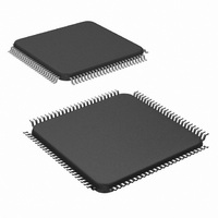
LM9833CCVJD/NOPB National Semiconductor, LM9833CCVJD/NOPB Datasheet - Page 31

LM9833CCVJD/NOPB
Manufacturer Part Number
LM9833CCVJD/NOPB
Description
IC USB IMAGE SCAN 48BIT 100-TOFP
Manufacturer
National Semiconductor
Datasheet
1.LM9833CCVJDNOPB.pdf
(42 pages)
Specifications of LM9833CCVJD/NOPB
Number Of Bits
16
Number Of Channels
3
Voltage - Supply, Analog
5V
Voltage - Supply, Digital
4.5 V ~ 5.5 V
Package / Case
100-TQFP, 100-VQFP
Lead Free Status / RoHS Status
Lead free / RoHS Compliant
Power (watts)
-
Other names
*LM9833CCVJD
*LM9833CCVJD/NOPB
LM9833CCVJD
*LM9833CCVJD/NOPB
LM9833CCVJD
Applications Information
should therefore be avoided. Bits 4 of register 3 is also read only,
however it is OK to write to register 3. All of the remaining config-
uration registers can be read from and written to using this proto-
col.
Registers 03-06 (the Dataport), 2A-27 (Illumination), 38-3D
(Static Gain and Offset), 42 (Offset and Gain Source, bits 0-2), 45
(Stepper Motor Status), and 58-5B (Paper Sense and Misc. I/O)
may be written to while the chip is in the Idle state. The LM9833
must be in Soft Reset mode to write all other configuration regis-
ters (see 10.2 Soft Reset).
6.1 The DataPort: Reading and Writing to Gamma, Offset,
and Gain Memory
Because the gamma table and the shading and offset correction
blocks of RAM are very large, the LM9833 uses an indexed
method of reading and writing them, called the DataPort. Four
addresses in the Configuration Register are used to implement
this feature, as shown in Figure 38.
The DataPort allows the user to select a memory block (gamma,
gain coefficient, or offset coefficient) and color (red, green, or
blue) to be read from or written to, by writing to Configuration
Register Address 3.
The starting address of that block (usually 0) is written into the
DataPort Address register (at Configuration Register Addresses
4 and 5). Bit D6 of register 4 should also be set to a 0 or a 1 to
indicate whether the DataPort will be read from (D6 = 1) or written
to (D6 = 0) in subsequent operations. This is required so the
LM9833 can prefetch the data for faster access. The DataPort
Address is automatically incremented after every word (2 bytes)
of Offset, Shading, or Gamma data is read/written.
Once the memory block, color, and starting address are written, a
series of reads or writes to the DataPort will read from or write to
the selected memory block at maximum speed.
Registers 4 and 5 should always be written to after Register 3 has
been changed.
Reading and writing the DataPort should only be done when the
LM9833 is not scanning (Register 07 = 0).
6.1.1 DataPort Type and Color
These 3 bits determine which memory block (gamma, gain, or off-
Configuration
Register
Address
3
4
5
6
Figure 38: DataPort
DataPort
DataPort
DataPort
DataPort
Address
Address
Target/
(MSB)
Name
(LSB)
Color
(Continued)
b13 - b8
b7 - b0
b7 - b0
b3- b0
Bits
31
set coefficients, Figure 39) and which color of that memory block
(red, green, or blue, Figure 40) is to be read from or written to.
6.1.2 DataPort Address
This 14 bit register (at Configuration Register addresses 4 and 5)
determines what the starting address is for the read/write opera-
tion. This address is automatically incremented after every 2 byte
word read/write operation to the actual DataPort. For the gamma
table the range is 0 to 4093. For the Gain and Offset Coefficients
this range is 0 (corresponding the first valid pixel as programmed
in the Valid Pixels Start register) to 16383 (the maximum number
of image pixels). If reads or writes continue past 4093 or 16383,
the DataPort address counter wraps back around to 0 and contin-
ues counting.
6.1.3 DataPort
The DataPort is the 8 bit register (Configuration Register address
06) where the data is sequentially read from or written to. The for-
mats for Offset, Gain, and Gamma data are shown in Figures 41,
42, and 43.
b15 b14 b13 b12 b11 b10
b15 b14 b13 b12 b11 b10
b7
b7
b7
7
7
7
0
7
-
-
-
-
7
-
-
-
-
b6
b6
b6
6
6
6
0
6
-
-
-
-
6
-
-
-
-
b5
b5
b5
Figure 43: DataPort Gamma Format
5
5
5
0
Figure 39: DataPort Target Pointer
Figure 41: DataPort Offset Format
Figure 40: DataPort Color Pointer
Figure 42: DataPort Gain Format
5
-
-
-
-
5
-
-
-
-
b4
b4
b4
4
-
-
-
-
4
-
-
-
-
4
4
4
0
0
0
1
1
b11 b10
3
-
-
-
-
3
b3
b3
b3
3
3
3
0
1
0
1
-
-
-
-
2
2
b2
b2
b2
2
2
2
0
0
1
1
1
1
-
-
-
-
b9
b1
b9
b1
b9
b1
1
1
1
0
1
0
1
0
0
-
-
-
-
b8
b0
b8
b0
b8
b0
0
0
0
Undefined
Undefined
Gamma
www.national.com
Offset
Color
Green
Type
Gain
Blue
Second Byte
Second Byte
Second Byte
Red
First Byte
First Byte
First Byte
Type
Type
Type


