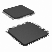
LM9833CCVJD/NOPB National Semiconductor, LM9833CCVJD/NOPB Datasheet - Page 20

LM9833CCVJD/NOPB
Manufacturer Part Number
LM9833CCVJD/NOPB
Description
IC USB IMAGE SCAN 48BIT 100-TOFP
Manufacturer
National Semiconductor
Datasheet
1.LM9833CCVJDNOPB.pdf
(42 pages)
Specifications of LM9833CCVJD/NOPB
Number Of Bits
16
Number Of Channels
3
Voltage - Supply, Analog
5V
Voltage - Supply, Digital
4.5 V ~ 5.5 V
Package / Case
100-TQFP, 100-VQFP
Lead Free Status / RoHS Status
Lead free / RoHS Compliant
Power (watts)
-
Other names
*LM9833CCVJD
*LM9833CCVJD/NOPB
LM9833CCVJD
*LM9833CCVJD/NOPB
LM9833CCVJD
Register Listing
Address
(NEW)
5F-68
6A-7F
TEST MODE SETTINGS
5B
5C
5D
5E
69
MISC I/O 5: Input or Output
MISC I/O 5: Polarity
(if configured as an input)
MISC I/O 5: Level/Edge sensitive
(if configured as an input)
MISC I/O 5: Output State
(if configured as an output)
Power On/USB Suspend Default: Output,
Logic High
MISC I/O 6: Input or Output
MISC I/O 6: Polarity
(if configured as an input)
MISC I/O 6: Level/Edge sensitive
(if configured as an input)
MISC I/O 6: Output State
(if configured as an output)
Power On/USB Suspend Default: Output,
Logic Low
ADC Output Code - MSB
ADC Output Code - LSB
ADC Test Mode
Pixel Processing Input Select
16 bit Counter Increment Select
(16 bit counter starts at 0, increments every
datapixel)
MCLK edge for AFE (Set this bit to 0)
CDS Signal
Reserved
Version Number
Reserved
(Continued)
Function
D
7
0
1
n n n n n n n n Used to force the input to the HDPI Divider to a known
n n n n n n n n
0
1
0 0 0 0 0 0 0 0 Write 00 to these registers
0 0 0 0 0 0 0 0 Write 00 to these registers
D
0
1
0
1
6
D
5
0
1
0 0
0 1
1 0
1 1
D
4
0
1
20
D
0
1
0 0
0 1
1 0
1 1
3
D
2
0
1
1 0 0
D
1
0
1
0 0 Normal Operation
0 1 Bypass AFE, Normal ADC Operation
1 0
1 1
D
0
0 The MISC I/O 5 pin is configured as an input.
1 The MISC I/O 5 pin is configured as an output.
A low input on MISC I/O 5 is True
A high input on MISC I/O 5 is True
Level sensitive: MISC I/O 5 State bit (in Status
Register) is set to a 1 if MISC I/O 5 is currently True.
Edge sensitive: MISC I/O 5 State bit (in Status
Register) is set to a 1 if MISC I/O 5 has been True
since the last time the Status Register was read.
The output of the MISC I/O 5 pin will be a logic low
(0V).
The output of the MISC I/O 5 pin will be a logic high
(5V).
The MISC I/O 6 pin is configured as an input.
The MISC I/O 6 pin is configured as an output.
A low input on MISC I/O 6 is True
A high input on MISC I/O 6 is True
Level sensitive: MISC I/O 6 State bit (in Status
Register) is set to a 1 if MISC I/O 6 is currently True.
Edge sensitive: MISC I/O 6 State bit (in Status
Register) is set to a 1 if MISC I/O 6 has been True
since the last time the Status Register was read.
The output of the MISC I/O 6 pin will be a logic low
(0V).
The output of the MISC I/O 6 pin will be a logic high
(5V).
value for digital tests
Bypass AFE, bypass ADC digital correction,
output uncorrected ADC MSB
Bypass AFE, bypass ADC digital correction,
output uncorrected ADC LSB
Normal Operation - ADC Output
Registers 5C and 5D
16 bit counter, reset at the start of every scan
16 bit counter, reset at the start of every line
Increments by 1
Increments by 4
Increments by 16
N/A
Rising
Falling
Normal Operation
CDS signal is output on LAMP
100 = LM9832 or LM9833
(011 = LM9831, 010 = LM9830)
Value
B
pin
www.national.com


