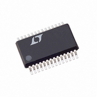
LTC2418CGN#PBF Linear Technology, LTC2418CGN#PBF Datasheet - Page 11

LTC2418CGN#PBF
Manufacturer Part Number
LTC2418CGN#PBF
Description
IC ADC 24BIT DIFF INPUT 28SSOP
Manufacturer
Linear Technology
Datasheet
1.LTC2418CGNPBF.pdf
(48 pages)
Specifications of LTC2418CGN#PBF
Number Of Bits
24
Sampling Rate (per Second)
7.5
Data Interface
MICROWIRE™, Serial, SPI™
Number Of Converters
1
Power Dissipation (max)
1mW
Voltage Supply Source
Single Supply
Operating Temperature
0°C ~ 70°C
Mounting Type
Surface Mount
Package / Case
28-SSOP (0.150", 3.95mm Width)
Number Of Elements
1
Resolution
24Bit
Architecture
Delta-Sigma
Sample Rate
0.008KSPS
Input Polarity
Bipolar
Input Type
Voltage
Rated Input Volt
±2.75V
Differential Input
Yes
Power Supply Requirement
Single
Single Supply Voltage (typ)
3.3/5V
Single Supply Voltage (min)
2.7V
Single Supply Voltage (max)
5.5V
Dual Supply Voltage (typ)
Not RequiredV
Dual Supply Voltage (min)
Not RequiredV
Dual Supply Voltage (max)
Not RequiredV
Integral Nonlinearity Error
14ppm of Vref
Operating Temp Range
0C to 70C
Operating Temperature Classification
Commercial
Mounting
Surface Mount
Pin Count
28
Package Type
SSOP N
Lead Free Status / RoHS Status
Lead free / RoHS Compliant
Available stocks
Company
Part Number
Manufacturer
Quantity
Price
APPLICATIO S I FOR ATIO
FU CTIO AL BLOCK DIAGRA
TEST CIRCUITS
CONVERTER OPERATION
Converter Operation Cycle
The LTC2414/LTC2418 are multichannel, low power, delta-
sigma analog-to-digital converters with an easy-to-use
4-wire serial interface (see Figure 1). Their operation is made
up of three states. The converter operating cycle begins with
the conversion, followed by the low power sleep state and
ends with the data input/output (see Figure 2). The 4-wire
interface consists of serial data input (SDI), serial data out-
put (SDO), serial clock (SCK) and chip select (CS).
Initially, the LTC2414 or LTC2418 performs a conversion.
Once the conversion is complete, the device enters the
sleep state. The part remains in the sleep state as long as
U
GND
U
V
CC
SDO
U
CH15
REF
REF
COM
CH0
CH1
Hi-Z TO V
V
V
1.69k
OL
OH
+
–
U
TO V
TO Hi-Z
•
•
•
OH
OH
MUX
241418 TA02
W
C
LOAD
= 20pF
IN
IN
+
–
∆Σ MODULATOR
U
–
DIFFERENTIAL
3RD ORDER
W
+
Figure 1
CS is HIGH. While in the sleep state, power consumption
is reduced by nearly two orders of magnitude. The conver-
sion result is held indefinitely in a static shift register while
the converter is in the sleep state.
Once CS is pulled LOW, the device exits the low power
mode and enters the data output state. If CS is pulled HIGH
before the first rising edge of SCK, the device returns to the
low power sleep mode and the conversion result is still
held in the internal static shift register. If CS remains LOW
after the first rising edge of SCK, the device begins output-
ting the conversion result and inputting channel selection
bits. Taking CS high at this point will terminate the data
output state and start a new conversion. The channel
selection control bits are shifted in through SDI from the
AUTOCALIBRATION
DECIMATING FIR
AND CONTROL
ADDRESS
LTC2414/LTC2418
SDO
OSCILLATOR
INTERFACE
INTERNAL
SERIAL
Hi-Z TO V
V
V
OH
OL
241418 F01
V
TO Hi-Z
TO V
CC
1.69k
241418 TA03
OL
C
OL
LOAD
= 20pF
F
(INT/EXT)
SDI
SCK
SDO
CS
O
11
241418fa


