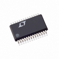
LTC2418CGN#PBF Linear Technology, LTC2418CGN#PBF Datasheet - Page 33

LTC2418CGN#PBF
Manufacturer Part Number
LTC2418CGN#PBF
Description
IC ADC 24BIT DIFF INPUT 28SSOP
Manufacturer
Linear Technology
Datasheet
1.LTC2418CGNPBF.pdf
(48 pages)
Specifications of LTC2418CGN#PBF
Number Of Bits
24
Sampling Rate (per Second)
7.5
Data Interface
MICROWIRE™, Serial, SPI™
Number Of Converters
1
Power Dissipation (max)
1mW
Voltage Supply Source
Single Supply
Operating Temperature
0°C ~ 70°C
Mounting Type
Surface Mount
Package / Case
28-SSOP (0.150", 3.95mm Width)
Number Of Elements
1
Resolution
24Bit
Architecture
Delta-Sigma
Sample Rate
0.008KSPS
Input Polarity
Bipolar
Input Type
Voltage
Rated Input Volt
±2.75V
Differential Input
Yes
Power Supply Requirement
Single
Single Supply Voltage (typ)
3.3/5V
Single Supply Voltage (min)
2.7V
Single Supply Voltage (max)
5.5V
Dual Supply Voltage (typ)
Not RequiredV
Dual Supply Voltage (min)
Not RequiredV
Dual Supply Voltage (max)
Not RequiredV
Integral Nonlinearity Error
14ppm of Vref
Operating Temp Range
0C to 70C
Operating Temperature Classification
Commercial
Mounting
Surface Mount
Pin Count
28
Package Type
SSOP N
Lead Free Status / RoHS Status
Lead free / RoHS Compliant
Available stocks
Company
Part Number
Manufacturer
Quantity
Price
APPLICATIO S I FOR ATIO
When external amplifiers are driving the LTC2414/
LTC2418, the ADC input referred system noise calculation
can be simplified by Figure 32. The noise of an amplifier
driving the LTC2414/LTC2418 input pin can be modeled
as a band limited white noise source. Its bandwidth can be
approximated by the bandwidth of a single pole lowpass
filter with a corner frequency f
tral density is n
selector, we can find on the y-axis the noise equivalent
bandwidth freq
width includes the band limiting effects of the ADC internal
calibration and filtering. The noise of the driving amplifier
referred to the converter input and including all these
effects can be calculated as N = n
noise (referred to the LTC2414/LTC2418 input) can now
be obtained by summing as square root of sum of squares
the three ADC input referred noise sources: the LTC2414/
LTC2418 internal noise (1µV), the noise of the IN
amplifier and the noise of the IN
If the F
f
x-axis is scaled by f
ratio f
decrease, but in the same time the LTC2414/LTC2418
noise floor rises and the noise contribution of the driving
amplifiers lose significance.
Normal Mode Rejection and Antialiasing
One of the advantages delta-sigma ADCs offer over con-
ventional ADCs is on-chip digital filtering. Combined with
a large oversampling ratio, the LTC2414/LTC2418 signifi-
cantly simplify antialiasing filter requirements.
The Sinc
mode rejection at all frequencies except DC and integer
multiples of the modulator sampling frequency (f
LTC2414/LTC2418’s autocalibration circuits further sim-
plify the antialiasing requirements by additional normal
mode signal filtering both in the analog and digital domain.
Independent of the operating mode, f
• f
the maximum output data rate. In the internal oscillator
mode with a 50Hz notch setting, f
60Hz notch setting f
mode, f
EOSC
OUTMAX
, Figure 32 can still be used for noise calculation if the
EOSC
O
S
pin is driven by an external oscillator of frequency
4
= f
digital filter provides greater than 120dB normal
where f
/153600, the Figure 32 plot accuracy begins to
EOSC
i
i
of the input driving amplifier. This band-
. From Figure 32, using f
/10.
N
in the notch frequency and f
U
S
EOSC
= 15360Hz. In the external oscillator
/153600. For large values of the
U
i
. The amplifier noise spec-
i
–
• √freq
S
driving amplifier.
W
= 12800Hz and with a
S
i
= 256 • f
. The total system
i
as the x-axis
U
OUTMAX
N
+
S
= 2048
driving
). The
is
Figure 32. Input Referred Noise Equivalent Bandwidth
of an Input Connected White Noise Source
Figure 34. Input Normal Mode Rejection, Internal
Oscillator and 60Hz Notch or External Oscillator
–100
–110
–120
–10
–20
–30
–40
–50
–60
–70
–80
–90
0
Figure 33. Input Normal Mode Rejection,
Internal Oscillator and 50Hz Notch
0
DIFFERENTIAL INPUT SIGNAL FREQUENCY (Hz)
–100
–110
–120
100
–10
–20
–30
–40
–50
–60
–70
–80
–90
0.1
10
f
S
1
0
0.1
0 f
DIFFERENTIAL INPUT SIGNAL FREQUENCY (Hz)
2f
S
S
INPUT NOISE SOURCE SINGLE POLE
F
3f
1
O
2f
LTC2414/LTC2418
S
EQUIVALENT BANDWIDTH (Hz)
= HIGH
S
4f
3f
S
10
S
4f
5f
S
S
100
5f
6f
F
F
S
O
O
S
6f
= LOW
= HIGH
7f
S
1k
S
7f
S
8f
8f
S
10k 100k
S
2414/18 F34
9f
9f
S
S
10f
10f
2414/18 F33
S
S
2414/18 F32
11f
F
F
f
EOSC
O
O
S
= LOW OR
= EXTERNAL
1M
12f
OSCILLATOR,
= 10 • f
S
33
S
241418fa


