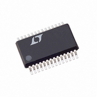
LTC2418CGN#PBF Linear Technology, LTC2418CGN#PBF Datasheet - Page 21

LTC2418CGN#PBF
Manufacturer Part Number
LTC2418CGN#PBF
Description
IC ADC 24BIT DIFF INPUT 28SSOP
Manufacturer
Linear Technology
Datasheet
1.LTC2418CGNPBF.pdf
(48 pages)
Specifications of LTC2418CGN#PBF
Number Of Bits
24
Sampling Rate (per Second)
7.5
Data Interface
MICROWIRE™, Serial, SPI™
Number Of Converters
1
Power Dissipation (max)
1mW
Voltage Supply Source
Single Supply
Operating Temperature
0°C ~ 70°C
Mounting Type
Surface Mount
Package / Case
28-SSOP (0.150", 3.95mm Width)
Number Of Elements
1
Resolution
24Bit
Architecture
Delta-Sigma
Sample Rate
0.008KSPS
Input Polarity
Bipolar
Input Type
Voltage
Rated Input Volt
±2.75V
Differential Input
Yes
Power Supply Requirement
Single
Single Supply Voltage (typ)
3.3/5V
Single Supply Voltage (min)
2.7V
Single Supply Voltage (max)
5.5V
Dual Supply Voltage (typ)
Not RequiredV
Dual Supply Voltage (min)
Not RequiredV
Dual Supply Voltage (max)
Not RequiredV
Integral Nonlinearity Error
14ppm of Vref
Operating Temp Range
0C to 70C
Operating Temperature Classification
Commercial
Mounting
Surface Mount
Pin Count
28
Package Type
SSOP N
Lead Free Status / RoHS Status
Lead free / RoHS Compliant
Available stocks
Company
Part Number
Manufacturer
Quantity
Price
(EXTERNAL)
APPLICATIO S I FOR ATIO
External Serial Clock, 3-Wire I/O
This timing mode utilizes a 3-wire serial I/O interface. The
conversion result is shifted out of the device by an exter-
nally generated serial clock (SCK) signal, see Figure 7. CS
may be permanently tied to ground, simplifying the user
interface or isolation barrier.
The external serial clock mode is selected at the end of the
power-on reset (POR) cycle. The POR cycle is concluded
typically 1ms after V
level applied to SCK at this time determines if SCK is
internal or external. SCK must be driven LOW prior to the
end of POR in order to enter the external serial clock timing
mode.
Since CS is tied LOW, the end-of-conversion (EOC) can be
continuously monitored at the SDO pin during the convert
and sleep states. EOC may be used as an interrupt to an
external controller indicating the conversion result is
ready. EOC = 1 while the conversion is in progress and
EOC = 0 once the conversion ends. On the falling edge of
EOC, the conversion result is loaded into an internal static
shift register. The input data is then shifted in via the SDI
pin on the rising edge of SCK (including the first rising
edge) and the output data is shifted out of the SDO pin on
SDO
SCK
SDI
CS
CONVERSION
DON’T CARE
U
CC
exceeds approximately 2V. The
U
BIT 31
(1)
EOC
W
BIT 30
(0)
Figure 7. External Serial Clock, CS = 0 Operation
EN
BIT 29
SIG
0.1V TO V
REFERENCE
U
ANALOG
INPUTS
VOLTAGE
SGL
BIT 28
1µF
2.7V TO 5.5V
MSB
CC
•
•
•
•
•
•
11
12
21
28
10
9
1
8
ODD/
SIGN
BIT 27
V
REF
REF
CH0
CH7
CH8
CH15
COM
CC
•
•
•
•
•
•
LTC2414/
LTC2418
+
–
each falling edge of SCK. EOC can be latched on the first
rising edge of SCK. On the 32nd falling edge of SCK, SDO
goes HIGH (EOC = 1) indicating a new conversion has
begun.
Internal Serial Clock, Single Cycle Operation
This timing mode uses an internal serial clock to shift out
the conversion result and a CS signal to monitor and
control the state of the conversion cycle, see Figure 8.
In order to select the internal serial clock timing mode, the
serial clock pin (SCK) must be floating (Hi-Z) or pulled
HIGH prior to the falling edge of CS. The device will not
enter the internal serial clock mode if SCK is driven LOW
on the falling edge of CS. An internal weak pull-up resistor
is active on the SCK pin during the falling edge of CS;
therefore, the internal serial clock timing mode is auto-
matically selected if SCK is not externally driven.
The serial data output pin (SDO) is Hi-Z as long as CS is
HIGH. At any time during the conversion cycle, CS may be
pulled LOW in order to monitor the state of the converter.
Once CS is pulled LOW, SCK goes LOW and EOC is output
to the SDO pin. EOC = 1 while a conversion is in progress
and EOC = 0 if the device is in the sleep state.
GND
SDO
SCK
A2
BIT 26
SDI
CS
F
O
DATA OUTPUT
17
15
20
18
19
16
BIT 25
A1
3-WIRE
SPI INTERFACE
V
CC
= 50Hz REJECTION
= EXTERNAL OSCILLATOR
= 60Hz REJECTION
A0
BIT 24
LTC2414/LTC2418
DON’T CARE
BIT 6
LSB
PARITY
BIT 0
CONVERSION
21
241418fa
241418 F07


