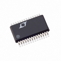
LTC2418CGN#PBF Linear Technology, LTC2418CGN#PBF Datasheet - Page 6

LTC2418CGN#PBF
Manufacturer Part Number
LTC2418CGN#PBF
Description
IC ADC 24BIT DIFF INPUT 28SSOP
Manufacturer
Linear Technology
Datasheet
1.LTC2418CGNPBF.pdf
(48 pages)
Specifications of LTC2418CGN#PBF
Number Of Bits
24
Sampling Rate (per Second)
7.5
Data Interface
MICROWIRE™, Serial, SPI™
Number Of Converters
1
Power Dissipation (max)
1mW
Voltage Supply Source
Single Supply
Operating Temperature
0°C ~ 70°C
Mounting Type
Surface Mount
Package / Case
28-SSOP (0.150", 3.95mm Width)
Number Of Elements
1
Resolution
24Bit
Architecture
Delta-Sigma
Sample Rate
0.008KSPS
Input Polarity
Bipolar
Input Type
Voltage
Rated Input Volt
±2.75V
Differential Input
Yes
Power Supply Requirement
Single
Single Supply Voltage (typ)
3.3/5V
Single Supply Voltage (min)
2.7V
Single Supply Voltage (max)
5.5V
Dual Supply Voltage (typ)
Not RequiredV
Dual Supply Voltage (min)
Not RequiredV
Dual Supply Voltage (max)
Not RequiredV
Integral Nonlinearity Error
14ppm of Vref
Operating Temp Range
0C to 70C
Operating Temperature Classification
Commercial
Mounting
Surface Mount
Pin Count
28
Package Type
SSOP N
Lead Free Status / RoHS Status
Lead free / RoHS Compliant
Available stocks
Company
Part Number
Manufacturer
Quantity
Price
LTC2414/LTC2418
TI I G CHARACTERISTICS
range, otherwise specifications are at T
SYMBOL
t
t2
t3
t4
t
t
t
t
Note 1: Absolute Maximum Ratings are those values beyond which the
life of the device may be impaired.
Note 2: All voltage values are with respect to GND.
Note 3: V
V
V
and negative input respectively.
Note 4: F
source with f
Note 5: Guaranteed by design, not subject to test.
Note 6: Integral nonlinearity is defined as the deviation of a code from
a straight line passing through the actual endpoints of the transfer
curve. The deviation is measured from the center of the quantization
band.
Note 7: F
(external oscillator).
6
1
KQMAX
KQMIN
t
t
7
8
5
6
REF
INCM
W
= REF
= (IN
O
O
U
CC
+
pin tied to GND or to V
= 0V (internal oscillator) or f
+
= 2.7V to 5.5V unless otherwise specified.
– REF
EOSC
+ IN
PARAMETER
CS ↓ to SDO Low
CS ↑ to SDO High Z
CS ↓ to SCK ↓
CS ↓ to SCK ↑
SCK ↓ to SDO Valid
SDO Hold After SCK ↓
SCK Set-Up Before CS ↓
SCK Hold After CS ↓
SDI Setup Before SCK↑
SDI Hold After SCK↑
–
= 153600Hz unless otherwise specified.
)/2, IN
–
, V
REFCM
+
and IN
= (REF
–
CC
are defined as the selected positive
+
or to external conversion clock
+ REF
EOSC
A
–
)/2; V
= 153600Hz ±2%
= 25°C. (Note 3)
IN
CONDITIONS
(Note 10)
(Note 9)
(Note 5)
(Note 5)
(Note 5)
= IN
+
The
– IN
●
–
,
denotes specifications which apply over the full operating temperature
Note 8: F
(external oscillator).
Note 9: The converter is in external SCK mode of operation such that
the SCK pin is used as digital input. The frequency of the clock signal
driving SCK during the data output is f
Note 10: The converter is in internal SCK mode of operation such that
the SCK pin is used as digital output. In this mode of operation the
SCK pin has a total equivalent load capacitance C
Note 11: The external oscillator is connected to the F
oscillator frequency, f
Note 12: The converter uses the internal oscillator.
F
Note 13: The output noise includes the contribution of the internal
calibration operations.
Note 14: Guaranteed by design and test correlation.
O
= 0V or F
O
= V
O
= V
CC
(internal oscillator) or f
CC
.
EOSC
●
●
●
●
●
●
●
●
●
●
, is expressed in kHz.
MIN
100
100
50
15
50
0
0
0
ESCK
EOSC
TYP
and is expressed in kHz.
= 128000Hz ±2%
LOAD
O
MAX
200
200
200
220
= 20pF.
pin. The external
50
241418fa
UNITS
ns
ns
ns
ns
ns
ns
ns
ns
ns
ns


