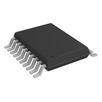
AD7328BRUZ Analog Devices Inc, AD7328BRUZ Datasheet - Page 13

AD7328BRUZ
Manufacturer Part Number
AD7328BRUZ
Description
IC ADC 12BIT+ SAR 8CHAN 20TSSOP
Manufacturer
Analog Devices Inc
Specifications of AD7328BRUZ
Data Interface
DSP, MICROWIRE™, QSPI™, Serial, SPI™
Design Resources
Using AD7328 in Appls with Single-Ended Industrial-Level Signals (CN0047)
Number Of Bits
12
Sampling Rate (per Second)
1M
Number Of Converters
1
Power Dissipation (max)
30mW
Voltage Supply Source
Dual ±
Operating Temperature
-40°C ~ 85°C
Mounting Type
Surface Mount
Package / Case
20-TSSOP (0.173", 4.40mm Width)
Resolution (bits)
13bit
Sampling Rate
1MSPS
Input Channel Type
Pseudo Differential, Single Ended
Supply Current
900µA
Digital Ic Case Style
TSSOP
No. Of Pins
20
Lead Free Status / RoHS Status
Lead free / RoHS Compliant
For Use With
EVAL-AD7328CBZ - BOARD EVALUATION FOR AD7328
Lead Free Status / Rohs Status
RoHS Compliant part
Electrostatic Device
Available stocks
Company
Part Number
Manufacturer
Quantity
Price
Part Number:
AD7328BRUZ
Manufacturer:
ADI/亚德诺
Quantity:
20 000
Company:
Part Number:
AD7328BRUZ-REEL7
Manufacturer:
ALLEGRO
Quantity:
1 200
TERMINOLOGY
Differential Nonlinearity
This is the difference between the measured and the ideal 1 LSB
change between any two adjacent codes in the ADC.
Integral Nonlinearity
This is the maximum deviation from a straight line passing
through the endpoints of the ADC transfer function. The
endpoints of the transfer function are zero scale (a point 1 LSB
below the first code transition) and full scale (a point 1 LSB above
the last code transition).
Offset Error
This applies to straight binary output coding. It is the deviation
of the first code transition (00 ... 000) to (00 ... 001) from the
ideal, that is, AGND + 1 LSB.
Offset Error Match
This is the difference in offset error between any two input
channels.
Gain Error
This applies to straight binary output coding. It is the deviation
of the last code transition (111 ... 110) to (111 ... 111) from the
ideal (that is, 4 × V
after adjusting for the offset error.
Gain Error Match
This is the difference in gain error between any two input channels.
Bipolar Zero Code Error
This applies when using twos complement output coding and a
bipolar analog input. It is the deviation of the midscale transition
(all 1s to all 0s) from the ideal input voltage, that is, AGND − 1 LSB.
Bipolar Zero Code Error Match
This refers to the difference in bipolar zero code error between
any two input channels.
Positive Full-Scale Error
This applies when using twos complement output coding and
any of the bipolar analog input ranges. It is the deviation of the
last code transition (011 … 110) to (011 … 111) from the ideal
(that is, 4 × V
adjusting for the bipolar zero code error.
Positive Full-Scale Error Match
This is the difference in positive full-scale error between any
two input channels.
REF
− 1 LSB, 2 × V
REF
− 1 LSB, 2 × V
REF
− 1 LSB, V
REF
− 1 LSB, V
REF
− 1 LSB) after
REF
− 1 LSB)
Rev. B | Page 13 of 36
Negative Full-Scale Error
This applies when using twos complement output coding and
any of the bipolar analog input ranges. This is the deviation of
the first code transition (10 … 000) to (10 … 001) from the ideal
(that is, −4 × V
after adjusting for the bipolar zero code error.
Negative Full-Scale Error Match
This is the difference in negative full-scale error between any
two input channels.
Track-and-Hold Acquisition Time
The track-and-hold amplifier returns to track mode after the
14
time required for the output of the track-and-hold amplifier to
reach its final value, within ±½ LSB, after the end of a conversion.
For the ±2.5 V range, the specified acquisition time is the time
required for the track-and-hold amplifier to settle to within ±1 LSB.
Signal-to-Noise-and-Distortion Ratio
This is the measured ratio of signal to (noise + distortion) at
the output of the ADC. The signal is the rms amplitude of the
fundamental. Noise is the sum of all nonfundamental signals up
to half the sampling frequency (f
dependent on the number of quantization levels in the digitization
process. The more levels, the smaller the quantization noise.
Theoretically, the signal-to-noise-and-distortion ratio for an
ideal N-bit converter with a sine wave input is given by
For a 13-bit converter, this is 80.02 dB.
Total Harmonic Distortion
Total harmonic distortion (THD) is the ratio of the rms sum of
harmonics to the fundamental. For the AD7328, it is defined as
where V
V
sixth harmonics.
Peak Harmonic or Spurious Noise
Peak harmonic or spurious noise is defined as the ratio of the
rms value of the next largest component in the ADC output
spectrum (up to f
fundamental. Normally, the value of this specification is
determined by the largest harmonic in the spectrum, but for
ADCs where the harmonics are buried in the noise floor, the
largest harmonic could be a noise peak.
4
th
, V
SCLK rising edge. Track-and-hold acquisition time is the
Signal to (Noise + Distortion) = (6.02 N + 1.76) dB
THD
5
, and V
1
is the rms amplitude of the fundamental, and V
(
dB
6
)
are the rms amplitudes of the second through the
REF
=
S
20
+ 1 LSB, −2 × V
/2, excluding dc) to the rms value of the
log
V
2
2
+
V
S
/2), excluding dc. The ratio is
3
REF
2
+
+ 1 LSB, −V
V
V
1
4
2
+
V
5
2
+
REF
V
6
AD7328
+ 1 LSB)
2
2
, V
3
,


