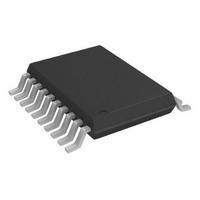
AD7328BRUZ Analog Devices Inc, AD7328BRUZ Datasheet - Page 22

AD7328BRUZ
Manufacturer Part Number
AD7328BRUZ
Description
IC ADC 12BIT+ SAR 8CHAN 20TSSOP
Manufacturer
Analog Devices Inc
Specifications of AD7328BRUZ
Data Interface
DSP, MICROWIRE™, QSPI™, Serial, SPI™
Design Resources
Using AD7328 in Appls with Single-Ended Industrial-Level Signals (CN0047)
Number Of Bits
12
Sampling Rate (per Second)
1M
Number Of Converters
1
Power Dissipation (max)
30mW
Voltage Supply Source
Dual ±
Operating Temperature
-40°C ~ 85°C
Mounting Type
Surface Mount
Package / Case
20-TSSOP (0.173", 4.40mm Width)
Resolution (bits)
13bit
Sampling Rate
1MSPS
Input Channel Type
Pseudo Differential, Single Ended
Supply Current
900µA
Digital Ic Case Style
TSSOP
No. Of Pins
20
Lead Free Status / RoHS Status
Lead free / RoHS Compliant
For Use With
EVAL-AD7328CBZ - BOARD EVALUATION FOR AD7328
Lead Free Status / Rohs Status
RoHS Compliant part
Electrostatic Device
Available stocks
Company
Part Number
Manufacturer
Quantity
Price
Part Number:
AD7328BRUZ
Manufacturer:
ADI/亚德诺
Quantity:
20 000
Company:
Part Number:
AD7328BRUZ-REEL7
Manufacturer:
ALLEGRO
Quantity:
1 200
AD7328
CONTROL REGISTER
The control register is used to select the analog input channel, analog input configuration, reference, coding, and power mode. The control
register is a write-only, 12-bit register. Data loaded on the DIN line corresponds to the AD7328 configuration for the next conversion. If the
sequence register is being used, data should be loaded into the control register after the range registers and the sequence register have been
initialized. The bit functions of the control register are described in Table 9 (the power-up status of all bits is 0).
MSB
15
Write
Table 9. Control Register Details
Bit
12, 11, 10
9, 8
7, 6
5
4
3, 2
1
The eight analog input channels can be configured as seven pseudo differential analog inputs, four pseudo differential inputs, four true
differential input pairs, or eight single-ended analog inputs.
Table 10. Analog Input Configuration Selection
ADD2
0
0
0
0
1
1
1
1
Channel Address Bits
14
Register
Select 1
ADD1
0
0
1
1
0
0
1
1
Mnemonic
ADD2, ADD1,
ADD0
Mode 1, Mode 0
PM1, PM0
Coding
REF
SEQ1/SEQ2
Weak/Three-State
ADD0
0
1
0
1
0
1
0
1
13
Register
Select 2
7 Pseudo Differential I/Ps
V
V
V
V
V
V
V
V
(Mode 1 = 1, Mode 0 = 1)
IN
IN
IN
IN
IN
IN
IN
IN
12
ADD2
Temperature indicator
0
1
2
3
4
5
6
+
Description
These three channel address bits are used to select the analog input channel for the next conversion if the
sequencer is not being used. If the sequencer is being used, the three channel address bits are used to
select the final channel in a consecutive sequence.
These two mode bits are used to select the configuration of the eight analog input pins, V
pins are used in conjunction with the channel address bits. On the AD7328, the analog inputs can be configured
as eight single-ended inputs, four fully differential input pairs, four pseudo differential inputs, or seven
pseudo differential inputs (see Table 10).
The power management bits are used to select different power mode options on the AD7328 (see Table 11).
This bit is used to select the type of output coding that the AD7328 uses for the next conversion result.
If coding = 0, the output coding is twos complement. If coding = 1, the output coding is straight binary.
When operating in sequence mode, the output coding for each channel is the value written to the coding
bit during the last write to the control register.
The reference bit is used to enable or disable the internal reference. If REF = 0, the external reference is
enabled and used for the next conversion, and the internal reference is disabled. If REF = 1, the internal ref-
erence is used for the next conversion. When operating in sequence mode, the reference used for each
channel is the value written to the REF bit during the last write to the control register.
The Sequence 1 and Sequence 2 bits are used to control the operation of the sequencer (see Table 12).
This bit selects the state of the DOUT line at the end of the current serial transfer. If the bit is set to 1, the
DOUT line is weakly driven to Channel Address Bit ADD2 of the following conversion. If this bit is set to 0,
DOUT returns to three-state at the end of the serial transfer (see the Serial Interface section).
11
ADD1
V
V
V
V
V
V
V
V
IN
IN
IN
IN
IN
IN
IN
IN
7
7
7
7
7
7
7
−
10
ADD0
9
Mode 1
(Mode 1 = 1, Mode 0 = 0)
V
V
V
V
V
V
V
V
V
4 Fully Differential I/Ps
IN
IN
IN
IN
IN
IN
IN
IN
IN
0
0
2
2
4
4
6
6
+
Rev. B | Page 22 of 36
8
Mode 0
V
V
V
V
V
V
V
V
V
IN
IN
IN
IN
IN
IN
IN
IN
IN
1
1
3
3
5
5
7
7
−
7
PM1
6
PM0
4 Pseudo Differential I/Ps
V
V
V
V
V
V
V
V
V
(Mode 1 = 0, Mode 0 = 1)
IN
IN
IN
IN
IN
IN
IN
IN
IN
0
0
2
2
4
4
6
6
+
5
Coding
4
REF
V
V
V
V
V
V
V
V
V
IN
IN
IN
IN
IN
IN
IN
IN
IN
1
1
3
3
5
5
7
7
−
3
SEQ1
2
SEQ2
(Mode 1 = 0, Mode 0 = 0)
V
V
V
V
V
V
V
V
V
IN
IN
IN
IN
IN
IN
IN
IN
IN
8 Single-Ended I/Ps
0
1
2
3
4
5
6
7
+
1
Weak/
Three-State
IN
0 to V
V
AGND
AGND
AGND
AGND
AGND
AGND
AGND
AGND
IN
IN
−
7. These
LSB
0
0


