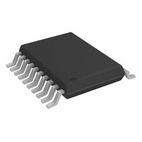
AD7328BRUZ Analog Devices Inc, AD7328BRUZ Datasheet - Page 21

AD7328BRUZ
Manufacturer Part Number
AD7328BRUZ
Description
IC ADC 12BIT+ SAR 8CHAN 20TSSOP
Manufacturer
Analog Devices Inc
Specifications of AD7328BRUZ
Data Interface
DSP, MICROWIRE™, QSPI™, Serial, SPI™
Design Resources
Using AD7328 in Appls with Single-Ended Industrial-Level Signals (CN0047)
Number Of Bits
12
Sampling Rate (per Second)
1M
Number Of Converters
1
Power Dissipation (max)
30mW
Voltage Supply Source
Dual ±
Operating Temperature
-40°C ~ 85°C
Mounting Type
Surface Mount
Package / Case
20-TSSOP (0.173", 4.40mm Width)
Resolution (bits)
13bit
Sampling Rate
1MSPS
Input Channel Type
Pseudo Differential, Single Ended
Supply Current
900µA
Digital Ic Case Style
TSSOP
No. Of Pins
20
Lead Free Status / RoHS Status
Lead free / RoHS Compliant
For Use With
EVAL-AD7328CBZ - BOARD EVALUATION FOR AD7328
Lead Free Status / Rohs Status
RoHS Compliant part
Electrostatic Device
Available stocks
Company
Part Number
Manufacturer
Quantity
Price
Part Number:
AD7328BRUZ
Manufacturer:
ADI/亚德诺
Quantity:
20 000
Company:
Part Number:
AD7328BRUZ-REEL7
Manufacturer:
ALLEGRO
Quantity:
1 200
REGISTERS
The AD7328 has four programmable registers: the control register, sequence register, Range Register 1, and Range Register 2. These
registers are write-only registers.
ADDRESSING REGISTERS
A serial transfer on the AD7328 consists of 16 SCLK cycles. The three MSBs on the DIN line during the 16 SCLK transfer are decoded to
determine which register is addressed. The three MSBs consist of the write bit, Register Select 1 bit, and Register Select 2 bit. The register
select bits are used to determine which of the four on-board registers is selected. The write bit determines if the data on the DIN line
following the register select bits loads into the addressed register. If the write bit is 1, the bits load into the register addressed by the
register select bits. If the write bit is 0, the data on the DIN line does not load into any register.
Table 8. Decoding Register Select Bits and Write Bit
Write
0
1
1
1
1
Register Select 1
0
0
0
1
1
Register Select 2
0
0
1
0
1
Description
Data on the DIN line during this serial transfer is ignored.
This combination selects the control register. The subsequent 12 bits are loaded into
the control register.
This combination selects Range Register 1. The subsequent 8 bits are loaded into
Range Register 1.
This combination selects Range Register 2. The subsequent 8 bits are loaded into
Range Register 2.
This combination selects the sequence register. The subsequent 8 bits are loaded into
the sequence register.
Rev. B | Page 21 of 36
AD7328


