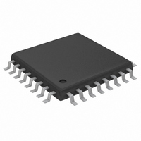
MAX1446EHJ+ Maxim Integrated Products, MAX1446EHJ+ Datasheet

MAX1446EHJ+
Specifications of MAX1446EHJ+
Related parts for MAX1446EHJ+
MAX1446EHJ+ Summary of contents
Page 1
... Operation) 5µA (Shutdown Mode) o Fully Differential Analog Input o Wide 2V o 400MHz -3dB Input Bandwidth o On-Chip 2.048V Precision Bandgap Reference o CMOS-Compatible Three-State Outputs o 32-Pin TQFP Package o Evaluation Kit Available (MAX1448 EV Kit) PART MAX1446EHJ+ MAX1446GHJ+ + Denotes a lead(Pb)-free/RoHS-compliant package. CLK IN+ T/H IN REFOUT ...
Page 2
... Spurious-Free Dynamic SFDR Range 2 _______________________________________________________________________________________ Continuous Power Dissipation (T 32-Pin TQFP (derate 18.7mW/°C above +70°C)......1495.3mW Operating Temperature Ranges: DD MAX1446EHJ+ .................................................-40°C to +85°C + 0.3V) MAX1446GHJ+...............................................-40°C to +105° 0.3V) Storage Temperature Range ............................-60°C to +150° 0.3V) Lead Temperature (soldering, 10s) .................................+300°C ...
Page 3
ELECTRICAL CHARACTERISTICS (continued 3.0V 2.7V; 0.1µF and 1.0µF capacitors from REFP, REFN, and COM to GND REFIN through a 10kΩ resistor unless otherwise noted. ≥+25°C guaranteed by production test, ...
Page 4
Low-Power ADC with Internal Reference ELECTRICAL CHARACTERISTICS (continued 3.0V 2.7V; 0.1µF and 1.0µF capacitors from REFP, REFN, and COM to GND REFIN through a 10kΩ resistor ...
Page 5
ELECTRICAL CHARACTERISTICS (continued 3.0V 2.7V; 0.1µF and 1.0µF capacitors from REFP, REFN, and COM to GND REFIN through a 10kΩ resistor unless otherwise noted. ≥+25°C guaranteed by production test, ...
Page 6
Low-Power ADC with Internal Reference (V = 3.0V 2.7V, internal reference, differential input at -0.5dBFS otherwise noted.) FFT PLOT (f = 7.5MHz, 8192-POINT FFT, IN DIFFERENTIAL INPUT) 0 SFDR = 72.2dBc -10 ...
Page 7
OV = 2.7V, internal reference, differential input at -0.5dBFS otherwise noted.) SIGNAL-TO-NOISE RATIO vs. ANALOG INPUT FREQUENCY (A = -0.5dBFS DIFFERENTIAL SINGLE-ENDED ...
Page 8
Low-Power ADC with Internal Reference (V = 3.0V 2.7V, internal reference, differential input at -0.5dBFS otherwise noted.) TOTAL HARMONIC DISTORTION vs. TEMPERATURE - 19.943MHz -0.5dBFS IN IN -64 ...
Page 9
OV = 2.7V, internal reference, differential input at -0.5dBFS otherwise noted.) DIGITAL SUPPLY CURRENT vs. TEMPERATURE 7.5MHz +105° -40 - ...
Page 10
Low-Power ADC with Internal Reference PIN NAME 1 REFN 2 COM 11, 14, 30 GND 6 IN+ 7 IN- 12 CLK 16–20 D9– ...
Page 11
Detailed Description The MAX1446 uses a 10-stage, fully differential, pipelined architecture (Figure 1) that allows for high- speed conversion while minimizing power consump- tion. Each sample moves through a pipeline stage every half-clock cycle. Counting the delay through the output ...
Page 12
Low-Power ADC with Internal Reference The MAX1446 provides three modes of reference oper- ation: • Internal reference mode • Buffered external reference mode • Unbuffered external reference mode In internal reference mode, the internal reference out- put ...
Page 13
AT -0.5dBFS CLOCK DUTY CYCLE (%) Figure 3a. SFDR vs. Clock Duty Cycle (Differential Input 12.5MHz AT -0.5dBFS ...
Page 14
Low-Power ADC with Internal Reference samples at the falling edge of the input clock. Output data is valid on the rising edge of the input clock. The output data has an internal latency of 5.5 clock cycles. ...
Page 15
INPUT MAX4108 0.1μF -5V 300Ω 300Ω Figure 7. Typical Application Circuit for Single-Ended to Differential Conversion 25Ω 22pF 0.1μ N. 2.2μF 0.1μ MINI-CIRCUITS ADT1–1WT 25Ω 22pF Figure ...
Page 16
Low-Power ADC with Internal Reference 3.3V 0.1μF 0.1μF 1 16.2kΩ 2 MAX6062 1μF 3 10Hz LOWPASS FILTER NOTE: ONE FRONT-END REFERENCE CIRCUIT DESIGN MAY BE USED WITH UP TO 1000 ADCs. Figure 10. Buffered External Reference Drives ...
Page 17
MAX6066 3 21.5kΩ 1μF 1.5V 3.3V 0.1μF 21.5kΩ MAX4254 POWER-SUPPLY BYPASSING. PLACE CAPACITOR AS CLOSE AS POSSIBLE TO THE OP AMP. 1.0V 21.5kΩ 21.5kΩ NOTE: ONE FRONT-END REFERENCE CIRCUIT DESIGN MAY BE USED WITH ...
Page 18
Low-Power ADC with Internal Reference ground pins could share the same ground plane if the ground plane is sufficiently isolated from any noisy, dig- ital systems ground plane (e.g., downstream output buffer or DSP ground plane). Route ...
Page 19
For the latest package outline information and land patterns www.maxim-ic.com/packages. PACKAGE TYPE 32 TQFP ______________________________________________________________________________________ 10-Bit, 60Msps, 3.0V, Low-Power ADC with Internal Reference Pin Configurations (continued) TOP VIEW REFN 1 COM ...
Page 20
... Maxim cannot assume responsibility for use of any circuitry other than circuitry entirely embodied in a Maxim product. No circuit patent licenses are implied. Maxim reserves the right to change the circuitry and specifications without notice at any time. 20 ____________________Maxim Integrated Products, 120 San Gabriel Drive, Sunnyvale, CA 94086 408-737-7600 © 2008 Maxim Integrated Products DESCRIPTION Maxim is a registered trademark of Maxim Integrated Products, Inc ...


