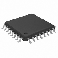
MAX1446EHJ+ Maxim Integrated Products, MAX1446EHJ+ Datasheet - Page 12

MAX1446EHJ+
Manufacturer Part Number
MAX1446EHJ+
Description
IC ADC 10BIT 60MSPS 32-TQFP
Manufacturer
Maxim Integrated Products
Datasheet
1.MAX1446EHJ.pdf
(20 pages)
Specifications of MAX1446EHJ+
Number Of Bits
10
Sampling Rate (per Second)
60M
Data Interface
Parallel
Number Of Converters
1
Voltage Supply Source
Single Supply
Operating Temperature
-40°C ~ 85°C
Mounting Type
Surface Mount
Package / Case
32-TQFP, 32-VQFP
Conversion Rate
60 MSPs
Resolution
10 bit
Snr
59.5 dB
Voltage Reference
2.048 V
Supply Voltage (max)
3.6 V
Supply Voltage (min)
2.7 V
Maximum Power Dissipation
1495.3 mW
Maximum Operating Temperature
+ 85 C
Mounting Style
SMD/SMT
Input Voltage
3 V
Minimum Operating Temperature
- 40 C
Lead Free Status / RoHS Status
Lead free / RoHS Compliant
10-Bit, 60Msps, 3.0V, Low-Power
ADC with Internal Reference
Table 1. MAX1446 Output Code for Differential Inputs
The MAX1446 provides three modes of reference oper-
ation:
•
•
•
In internal reference mode, the internal reference out-
put (REFOUT) can be tied to the REFIN pin through a
resistor (e.g., 10kΩ) or resistor-divider if an application
requires a reduced full-scale range. For stability pur-
poses, it is recommended to bypass REFIN with a
> 10nF capacitor to GND.
In buffered external reference mode, the reference volt-
age levels can be adjusted externally by applying a
stable and accurate voltage at REFIN. In this mode,
REFOUT may be left open or connected to REFIN
through a > 10kΩ resistor.
In unbuffered external reference mode, REFIN is con-
nected to GND, thereby deactivating the on-chip
buffers of REFP, COM, and REFN. With their buffers
shut down, these pins become high impedance and
can be driven by external reference sources.
The MAX1446 CLK input accepts CMOS-compatible
clock signals. Since the interstage conversion of the
device depends on the repeatability of the rising and
falling edges of the external clock, use a clock with low
jitter and fast rise and fall times (< 2ns). In particular,
sampling occurs on the falling edge of the clock signal,
mandating this edge to provide lowest possible jitter.
Any significant aperture jitter would limit the SNR per-
formance of the ADC as follows:
where f
t
*V
12
AJ
REFIN
Internal reference mode
Buffered external reference mode
Unbuffered external reference mode
is the time of the aperture jitter.
DIFFERENTIAL INPUT VOLTAGE*
______________________________________________________________________________________
= V
IN
REFP
SNR
represents the analog input frequency, and
- V
- V
V
V
- V
V
REF
REF
REF
REF
REF
= V
REF
=
× 511/512
× 510/512
20
× 511/512
× 512/512
REFN
× 1/512
0
× 1/512
×
log
⎛
⎜
⎝
2
× ×
π
Clock Input (CLK)
f
1
IN
×
t
AJ
⎞
⎟
⎠
Negative Full Scale + 1LSB
DIFFERENTIAL INPUT
Negative Full Scale
+Full Scale -1LSB
+Full Scale -2LSB
Bipolar Zero
+1LSB
-1LSB
Clock jitter is especially critical for undersampling
applications. The clock input should always be consid-
ered as an analog input and routed away from any ana-
log input or other digital signal lines.
The MAX1446 clock input operates with a voltage
threshold set to V
other than 50% must meet the specifications for high
and low periods as stated in the Electrical Character-
istics . See Figures 3a, 3b, 4a, and 4b for the relation-
ship between spurious-free dynamic range (SFDR),
signal-to-noise ratio (SNR), total harmonic distortion
(THD), or signal-to-noise plus distortion (SINAD) vs.
duty cycle.
All data outputs, D0 (LSB) through D9 (MSB), are
TTL/CMOS-logic compatible. There is a 5.5 clock-cycle
latency between any particular sample and its valid
output data. The output coding is straight offset binary
(Table 1). With OE and PD (power-down) high, the digi-
tal output enters a high-impedance state. If OE is held
low with PD high, the outputs are latched at the last
value prior to the power-down.
The capacitive load on the digital outputs D0–D9
should be kept as low as possible (< 15pF) to avoid
large digital currents that could feed back into the ana-
log portion of the MAX1446, degrading its dynamic per-
formance. The use of buffers on the ADC’s digital
outputs can further isolate the digital outputs from
heavy capacitive loads.
To further improve the dynamic performance of the
MAX1446 small series resistors (e.g., 100Ω) may be
added to the digital output paths, close to the ADC.
Figure 5 displays the timing relationship between out-
put enable and data output valid, as well as power-
down/wake-up and data output valid.
Figure 6 shows the relationship between the clock
input, analog input, and data output. The MAX1446
Output Enable ( OE ), Power-Down (PD),
System Timing Requirements
DD
/2. Clock inputs with a duty cycle
STRAIGHT OFFSET BINARY
and Output Data (D0–D9)
11 1111 1111
11 1111 1110
10 0000 0001
10 0000 0000
01 1111 1111
00 0000 0001
00 0000 0000


