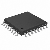
MAX1446EHJ+ Maxim Integrated Products, MAX1446EHJ+ Datasheet - Page 17

MAX1446EHJ+
Manufacturer Part Number
MAX1446EHJ+
Description
IC ADC 10BIT 60MSPS 32-TQFP
Manufacturer
Maxim Integrated Products
Datasheet
1.MAX1446EHJ.pdf
(20 pages)
Specifications of MAX1446EHJ+
Number Of Bits
10
Sampling Rate (per Second)
60M
Data Interface
Parallel
Number Of Converters
1
Voltage Supply Source
Single Supply
Operating Temperature
-40°C ~ 85°C
Mounting Type
Surface Mount
Package / Case
32-TQFP, 32-VQFP
Conversion Rate
60 MSPs
Resolution
10 bit
Snr
59.5 dB
Voltage Reference
2.048 V
Supply Voltage (max)
3.6 V
Supply Voltage (min)
2.7 V
Maximum Power Dissipation
1495.3 mW
Maximum Operating Temperature
+ 85 C
Mounting Style
SMD/SMT
Input Voltage
3 V
Minimum Operating Temperature
- 40 C
Lead Free Status / RoHS Status
Lead free / RoHS Compliant
The MAX1446 requires high-speed board layout design
techniques. Locate all bypass capacitors as close to
the device as possible, preferably on the same side as
the ADC, using surface-mount devices for minimum
inductance. Bypass V
two parallel 0.1µF ceramic capacitors and a 2.2µF
bipolar capacitor to GND. Follow the same rules to
bypass the digital supply (OV
boards with separated ground and power planes pro-
Figure 11. Unbuffered External Reference Drives Up to 32 ADCs
__________________and Board Layout
3.3V
NOTE: ONE FRONT-END REFERENCE CIRCUIT DESIGN MAY BE USED WITH UP TO 32 ADCs.
MAX4254 POWER-SUPPLY BYPASSING.
PLACE CAPACITOR AS CLOSE AS
POSSIBLE TO THE OP AMP.
MAX6066
0.1μF
3
1
0.1μF
3.3V
______________________________________________________________________________________
Grounding, Bypassing,
2
21.5kΩ
DD
1μF
, REFP, REFN, and COM with
21.5kΩ
21.5kΩ
21.5kΩ
21.5kΩ
DD
2.0V
) to OGND. Multilayer
1.5V
1.0V
10
3
2
5
6
9
10-Bit, 60Msps, 3.0V, Low-Power
1/4 MAX4252
1/4 MAX4252
1/4 MAX4252
4
11
4
11
4
11
ADC with Internal Reference
1
8
7
10μF
6V
10μF
6V
10μF
6V
3.3V
1.47kΩ
3.3V
1.47kΩ
3.3V
1.47kΩ
47Ω
47Ω
47Ω
1.0V AT -8mA
2.0V AT 8mA
1.5V AT 0mA
330μF
6V
330μF
330μF
duce the highest level of signal integrity. Consider
using a split ground plane arranged to match the physi-
cal location of the analog ground (GND) and the digital
output driver ground (OGND) on the ADC's package.
The two ground planes should be joined at a single
point so that the noisy digital ground currents do not
interfere with the analog ground plane. The ideal loca-
tion of this connection can be determined experimen-
tally at a point along the gap between the two ground
planes that produces optimum results. Make this con-
nection with a low-value, surface-mount resistor (1Ω to
5Ω), a ferrite bead, or a direct short. Alternatively, all
6V
6V
0.1μF
0.1μF
0.1μF
0.1μF
N.C.
N.C.
0.1μF
0.1μF
29
31
32
29
31
32
1
2
1
2
REFIN
REFP
REFN
COM
REFIN
REFP
REFN
COM
REFOUT
REFOUT
MAX1446
MAX1446
N = 32
N = 1
0.1μF
2.2μF
10V
17


