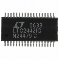
LTC2442IG#PBF Linear Technology, LTC2442IG#PBF Datasheet - Page 10

LTC2442IG#PBF
Manufacturer Part Number
LTC2442IG#PBF
Description
IC ADC 24BIT 4CH 36-SSOP
Manufacturer
Linear Technology
Datasheet
1.LTC2442CGPBF.pdf
(32 pages)
Specifications of LTC2442IG#PBF
Number Of Bits
24
Sampling Rate (per Second)
8k
Data Interface
MICROWIRE™, Serial, SPI™
Number Of Converters
1
Power Dissipation (max)
50mW
Voltage Supply Source
Single Supply
Operating Temperature
-40°C ~ 85°C
Mounting Type
Surface Mount
Package / Case
36-SSOP (0.200", 5.30mm Width)
Lead Free Status / RoHS Status
Lead free / RoHS Compliant
Available stocks
Company
Part Number
Manufacturer
Quantity
Price
APPLICATIO S I FOR ATIO
LTC2442
Once CS is pulled LOW, the device begins outputting the
conversion result. There is no latency in the conversion
result while operating in the 1X mode. The data output
corresponds to the conversion just performed. This result
is shifted out on the serial data out pin (SDO) under the
control of the serial clock (SCK). Data is updated on the
falling edge of SCK allowing the user to reliably latch
data on the rising edge of SCK (see Figure 3). The data
output state is concluded once 32 bits are read out of the
ADC or when CS is brought HIGH. In either scenario, the
device automatically initiates a new conversion and the
cycle repeats.
Through timing control of the CS, SCK and EXT pins,
the LTC2442 offers several fl exible modes of operation
(internal or external SCK). These various modes do not
require programming confi guration registers; moreover,
they do not disturb the cyclic operation described above.
These modes of operation are described in detail in the
Serial Interface Timing Modes section.
Ease of Use
The LTC2442 data output has no latency, fi lter settling delay
or redundant data associated with the conversion cycle
while operating in the 1X mode. There is a one-to-one cor-
respondence between the conversion and the output data.
Therefore, multiplexing multiple analog voltages is easy.
Speed/resolution adjustments may be made seamlessly
between two conversions without settling errors.
10
BUSY
SDO
SCK
SDI
CS
Hi-Z
1
U
BIT 31
EOC
1
2
BIT 30
Figure 3. SDI Speed/Resolution, Channel Selection, and Data Output Timing
U
“0”
0
3
BIT 29
SIG
EN
4
W
BIT 28 BIT 27 BIT 26 BIT 25 BIT 24 BIT 23 BIT 22 BIT 21
MSB
SGL
5
ODD
6
U
A2
7
A1
8
A0
The LTC2442 performs offset and full-scale calibrations
every conversion cycle. This calibration is transparent to
the user and has no effect on the cyclic operation described
above. The advantage of continuous calibration is extreme
stability of offset and full-scale readings with respect to
time, supply voltage change and temperature drift.
Power-Up Sequence
The LTC2442 automatically enters an internal reset state
when the power supply voltage V
proximately 2.2V. This feature guarantees the integrity
of the conversion result and of the serial interface mode
selection.
When the V
the converter creates an internal power-on-reset (POR)
signal with a duration of approximately 0.5ms. The POR
signal clears all internal registers. The conversion im-
mediately following a POR is performed on the input
channel SEL
1X mode. Following the POR signal, the LTC2442 starts
a normal conversion cycle and follows the succession of
states described above. The fi rst conversion result fol-
lowing POR is accurate within the specifi cations of the
device if the power supply voltage is restored within the
operating range (4.5V to 5.5V) before the end of the POR
time interval.
9
OSR3
10
OSR2
CC
11
+
OSR1
= CH0, SEL
voltage rises above this critical threshold,
12
BIT 20 BIT 19
OSR0 TWOX
13
–
= CH1 at an OSR = 256 in the
14
CC
BIT 0
32
drops below ap-
LSB
2442 F03
Hi-Z
2442f


