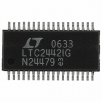
LTC2442IG#PBF Linear Technology, LTC2442IG#PBF Datasheet - Page 27

LTC2442IG#PBF
Manufacturer Part Number
LTC2442IG#PBF
Description
IC ADC 24BIT 4CH 36-SSOP
Manufacturer
Linear Technology
Datasheet
1.LTC2442CGPBF.pdf
(32 pages)
Specifications of LTC2442IG#PBF
Number Of Bits
24
Sampling Rate (per Second)
8k
Data Interface
MICROWIRE™, Serial, SPI™
Number Of Converters
1
Power Dissipation (max)
50mW
Voltage Supply Source
Single Supply
Operating Temperature
-40°C ~ 85°C
Mounting Type
Surface Mount
Package / Case
36-SSOP (0.200", 5.30mm Width)
Lead Free Status / RoHS Status
Lead free / RoHS Compliant
Available stocks
Company
Part Number
Manufacturer
Quantity
Price
APPLICATIO S I FOR ATIO
Low Power Operation
The integrated buffers have a supply current of 1mA total,
greatly reducing the total power consumption when the
ADC is operated at a low duty cycle. The typical approach
to driving a ΔΣ ADC is to use a high bandwidth ampli-
fi er that settles very quickly in response to the sampling
process at the ADC input. The LTC2442 approach is to use
an accurate, low bandwidth amplifi er that requires a load
capacitor for compensation. This capacitor also serves as
a charge reservoir during the sampling process, so the
disturbance at the ADC input is minimal. The amplifi er
only supplies the average sampling current that the ADC
draws, which is on the order of 50µA.
Scaling for Higher Input Voltages
The LTC2442 is ideally suited for applications with low-level,
differential signal with a common mode approximately
equal to mid-supply, such as strain gages and silicon
micromachined sensors. Other applications require scaling
a high voltage signal to the range of the ADC.
Figure 20 shows how to properly scale a bipolar, ground-
referred input voltage to drive the LTC2442. First, the
input must be level shifted so that it never exceeds the
LTC2442 supply rails. This is commonly done with an
U
U
W
U
instrumentation amplifi er or simple op-amp level shift
circuit. Rather than shift the analog input, the LTC2442
can run on ±2.5V supplies so that ground is centered in
the input range. This is equivalent to a perfect analog
level shift with no degradation in accuracy. The digital
signals are shifted from 0 to 5V logic to ±2.5V logic by a
very inexpensive 74HC4053 analog switch and the data
from the LTC2442 is shifted back to 0 to 5V logic by a
MMBT3904 transistor.
On both inputs, precision resistor networks scale the input
signal from ±10V to ±2.5V. CH0-1 is driven truly differen-
tially for maximum linearity, typically better than 3ppm,
however 3 resistors and an LTC2050HV autozero amplifi er
are required. The 8.88kΩ output resistor balances the offset
associated with the LTC2442’s bias current. The resistance
seen by CH0 is 4.44k and the offset at CH0 is also inverted
and appears at the output of the LTC2050HV.
CH2 to CH3 is driven single-ended, with CH3 tied to ground.
This degrades linearity slightly, but it is easier to implement
than a true differential drive. In this case the resistance at
CH3 should be equal to the resistance at CH2 or 7.5k. This
circuit is also suitable for signals that are always positive,
with the LTC2442 operating on a single 5V supply.
LTC2442
27
2442f


