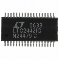
LTC2442IG#PBF Linear Technology, LTC2442IG#PBF Datasheet - Page 8

LTC2442IG#PBF
Manufacturer Part Number
LTC2442IG#PBF
Description
IC ADC 24BIT 4CH 36-SSOP
Manufacturer
Linear Technology
Datasheet
1.LTC2442CGPBF.pdf
(32 pages)
Specifications of LTC2442IG#PBF
Number Of Bits
24
Sampling Rate (per Second)
8k
Data Interface
MICROWIRE™, Serial, SPI™
Number Of Converters
1
Power Dissipation (max)
50mW
Voltage Supply Source
Single Supply
Operating Temperature
-40°C ~ 85°C
Mounting Type
Surface Mount
Package / Case
36-SSOP (0.200", 5.30mm Width)
Lead Free Status / RoHS Status
Lead free / RoHS Compliant
Available stocks
Company
Part Number
Manufacturer
Quantity
Price
LTC2442
PI FU CTIO S
MUXOUTA (Pin 27): Multiplexer Output. Must tie to +INA
amplifi er input (Pin 25).
COM (Pin 28): The common negative input (SEL
single ended multiplexer confi gurations. The voltage on
CH0-CH3 and COM pins can have any value between GND
–0.3V to V
inputs (SEL
= SEL
this input range, the converter produces unique over-range
and under-range output codes.
V
a 10µF tantalum capacitor in parallel with a 0.1µF ceramic
capacitor as close to the part as possible.
REF
The voltage on these pins can have any value between GND
and V
maintained more positive than the negative reference input,
REF
capacitor as close to the part as possible.
SDI (Pin 33): Serial Data Input. This pin is used to select
the speed, 1X or 2X mode, resolution and input channel
for the next conversion cycle. At initial power up, the de-
fault mode of operation is CH0-CH1, OSR of 256 and 1X
mode. The serial data input contains an enable bit which
determines if a new channel/speed is selected. If this bit is
low the following conversion remains at the same speed
and selected channel. The serial data input is applied to
8
CC
U
(Pin 29): Positive Supply Voltage. Bypass to GND with
–
+
, by at least 0.1V. Bypass to GND with 0.1µF Ceramic
(Pin 30), REF
CC
+
– SEL
as long as the reference positive input, REF
CC
U
+
and SEL
+0.3V. Within these limits, the two selected
–
) from –0.5 • V
–
(Pin 31): Differential Reference Input.
U
–
) provide a bipolar input range (V
REF
to 0.5 • V
REF
. Outside
–
) for all
+
, is
IN
the device under control of the serial clock (SCK) during
the data output cycle. The fi rst conversion following a new
channel/speed is valid.
F
trols the internal conversion clock. When F
to V
running at 9MHz. The conversion rate is determined by the
selected OSR such that t
(kHz). The fi rst digital fi lter null is located at 8/t
at OSR = 256 and 55Hz (Simultaneous 50Hz/60Hz at OSR
= 32768. This pin may be driven with a maximum external
clock of 10.24MHz resulting in a maximum 8kHz output
rate (OSR = 64, 2X mode).
CS (Pin 35): Active Low Chip Select. A LOW on this pin
enables the SDO digital output and wakes up the ADC.
Following each conversion the ADC automatically enters
the sleep mode and remains in this state as long as CS is
HIGH. A LOW-to-HIGH transition on CS during the Data
Output aborts the data transfer and starts a new conver-
sion.
SDO (Pin 36): Three-State Digital Output. During the data
output period, this pin is used as serial data output. When
the chip select CS is HIGH (CS = V
a high impedance state. During the conversion and sleep
periods, this pin is used as the conversion status output.
The conversion status can be observed by pulling CS LOW.
This signal is HIGH while the conversion is in progress
and goes LOW once the conversion is complete.
0
(Pin 34): Frequency Control Pin. Digital input that con-
CC
or GND, the converter uses its internal oscillator
CONV
(ms) = 40 • OSR + 170/f
CC
) the SDO pin is in
0
is connected
CONV
, 7kHz
OSC
2442f


