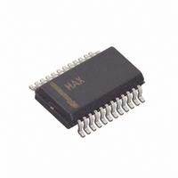
MAX1168BCEG+ Maxim Integrated Products, MAX1168BCEG+ Datasheet - Page 14

MAX1168BCEG+
Manufacturer Part Number
MAX1168BCEG+
Description
IC ADC 16BIT 200KSPS 24-QSOP
Manufacturer
Maxim Integrated Products
Datasheet
1.MAX1167BEEE.pdf
(30 pages)
Specifications of MAX1168BCEG+
Number Of Bits
16
Sampling Rate (per Second)
200k
Data Interface
MICROWIRE™, QSPI™, Serial, SPI™
Number Of Converters
1
Power Dissipation (max)
762mW
Voltage Supply Source
Analog and Digital
Operating Temperature
0°C ~ 70°C
Mounting Type
Surface Mount
Package / Case
24-QSOP
Lead Free Status / RoHS Status
Lead free / RoHS Compliant
The MAX1167/MAX1168 feature an SPI/QSPI/
MICROWIRE-compatible, 3-wire serial interface. The
MAX1167 digital interface consists of digital inputs CS,
SCLK, and DIN and outputs DOUT and EOC. The
MAX1167 operates in the following modes:
• SPI interface with external clock
• SPI interface with internal clock
• SPI interface with internal clock and scan mode
Multichannel, 16-Bit, 200ksps Analog-to-Digital
Converters
Figure 5. MAX1167 Typical Operating Circuit
Figure 7. Equivalent Input Circuit
Table 1. Command/Configuration/Control Register
14
AIN_
COMMAND
POWER-UP
ANALOG
INPUTS
STATE
+5V
+5V
______________________________________________________________________________________
R
DIN
DSON
C
MUX
MUX
BIT7 (MSB)
1μF
CH SEL2
TRACK
HOLD
C
0.1μF
SWITCH
0.1μF
0
REF
DV
CAPACITIVE
REF
AV
AIN0
AIN1
AIN2
AIN3
DIN
AGND
CH SEL1
DD
DD
C
HOLD
DAC
DAC
BIT6
Digital Interface
0
MAX1167
GND
TRACK
R
CH SEL0
REFCAP
IN
ZERO
DGND
AGND
AGND
SCLK
DOUT
BIT5
EOC
CS
0
AUTOZERO
RAIL
CS
SCLK
DOUT
EOC
0.1μF
SCAN1
BIT4
0
SCAN0
BIT3
In addition to the standard 3-wire serial interface modes,
the MAX1168 includes a DSPR input and a DSPX output
for communicating with DSPs in external clock mode and
a DSEL input to determine 8-bit-wide or 16-bit-wide data-
transfer mode. When not using the MAX1168 in the DSP
interface mode, connect DSPR to DV
unconnected.
Table 1 shows the contents of the command/configura-
tion/control register and the state of each bit after initial
power-up. Tables 2–6 define the control and configuration
of the device for each bit. Cycling the power supplies
resets the command/configuration/control register to the
power-on-reset default state.
A logic high on CS places the MAX1167/MAX1168 in
the shutdown mode chosen by the power-down bits,
and places DOUT in a high-impedance state. Drive CS
low to power up and enable the MAX1167/MAX1168
before starting a conversion. In internal reference
mode, allow 5ms for the shutdown internal reference
and/or buffer to wake and stabilize before starting a
conversion. In external reference mode (or if the inter-
nal reference is already on), no reference settling time
is needed after power-up.
Figure 6. MAX1168 T ypical Operating Circuit
0
Command/Configuration/Control Register
ANALOG
INPUTS
REF/PD_SEL1
+5V
+5V
DIN
8
16
BIT2
1
1μF
0.1μF
Initialization After Power-Up
0.1μF
REF/PD SEL0
DV
REF
AV
AIN0
AIN1
AIN2
AIN3
AIN4
AIN5
AIN6
AIN7
DIN
DSEL
DSPR
DD
DD
BIT1
MAX1168
1
GND
REFCAP
DD
DGND
DOUT
AGND
AGND
SCLK
DSPX
EOC
CS
and leave DSPX
INT/EXT CLK
BIT0 (LSB)
CS
SCLK
DSPX
DOUT
EOC
0.1μF
0


