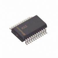
MAX1168BCEG+ Maxim Integrated Products, MAX1168BCEG+ Datasheet - Page 2

MAX1168BCEG+
Manufacturer Part Number
MAX1168BCEG+
Description
IC ADC 16BIT 200KSPS 24-QSOP
Manufacturer
Maxim Integrated Products
Datasheet
1.MAX1167BEEE.pdf
(30 pages)
Specifications of MAX1168BCEG+
Number Of Bits
16
Sampling Rate (per Second)
200k
Data Interface
MICROWIRE™, QSPI™, Serial, SPI™
Number Of Converters
1
Power Dissipation (max)
762mW
Voltage Supply Source
Analog and Digital
Operating Temperature
0°C ~ 70°C
Mounting Type
Surface Mount
Package / Case
24-QSOP
Lead Free Status / RoHS Status
Lead free / RoHS Compliant
ABSOLUTE MAXIMUM RATINGS
AV
DV
DGND to AGND.....................................................-0.3V to +0.3V
AIN_, REF, REFCAP to AGND..................-0.3V to (AV
SCLK, CS, DSEL, DSPR, DIN to DGND ...................-0.3V to +6V
DOUT, DSPX, EOC to DGND...................-0.3V to (DV
Maximum Current into Any Pin............................................50mA
Multichannel, 16-Bit, 200ksps Analog-to-Digital
Converters
ELECTRICAL CHARACTERISTICS
(AV
= +4.096V, T
Stresses beyond those listed under “Absolute Maximum Ratings” may cause permanent damage to the device. These are stress ratings only, and functional
operation of the device at these or any other conditions beyond those indicated in the operational sections of the specifications is not implied. Exposure to
absolute maximum rating conditions for extended periods may affect device reliability.
2
DC ACCURACY (Note 1)
Resolution
Relative Accuracy (Note 2)
Differential Nonlinearity
Transition Noise
Offset Error
Gain Error
Offset Drift
Gain Drift
DYNAMIC SPECIFICATIONS (1kHz sine wave, 4.096V
Signal-to-Noise Plus Distortion
Signal-to-Noise Ratio
Total Harmonic Distortion
Spurious-Free Dynamic Range
Full-Power Bandwidth
Full-Linear Bandwidth
Channel-to-Channel Isolation
CONVERSION RATE
Conversion Time
Acquisition Time
Serial Clock Frequency
DD
DD
DD
_______________________________________________________________________________________
to AGND .........................................................-0.3V to +6V
to DGND.........................................................-0.3V to +6V
= DV
PARAMETER
DD
A
= T
= +4.75V to +5.25V, f
MIN
to T
MAX
, unless otherwise noted. Typical values are at T
SYMBOL
SCLK
SINAD
t
SFDR
f
CONV
t
DNL
SNR
THD
SCLK
INL
ACQ
= 4.8MHz external clock (50% duty cycle), 24 clocks/conversion (200ksps), external V
MAX116_B
MAX116_B
(16 bit, no missing codes over temperature)
RMS
noise
(Note 3)
(Note 3)
-3dB point
SINAD > 85dB
(Note 4)
Internal clock, no data transfer,
single conversion (Note 5)
External clock
(Note 6)
External clock, data transfer and conversion
External clock, data transfer only
DD
DD
+ 0.3V)
+ 0.3V)
P-P
) (Note 1)
External reference
Internal reference
CONDITIONS
Continuous Power Dissipation (T
Operating Temperature Ranges
Maximum Junction Temperature .....................................+150°C
Storage Temperature Range .............................-65°C to +150°C
Lead Temperature (soldering, 10s) .................................+300°C
16-Pin QSOP (derate 8.3mW/°C above +70°C)...........667mW
24-Pin QSOP (derate 9.5mW/°C above +70°C)...........762mW
MAX116_ _ CE_ ..................................................0°C to +70°C
MAX116_ _ EE_ ...............................................-40°C to +85°C
A
= +25°C.)
16-bit
NMC
MIN
729
0.1
16
85
86
88
A
= +70°C)
±0.01
±1.8
+0.7
±0.1
±1.2
-100
TYP
88.5
88.5
5.52
3.75
101
0.7
0.8
10
96
1
4
+1.75
MAX
±0.2
7.07
±10
-88
4.8
±3
9
LSB
ppm/°C
ppm/°C
UNITS
%FSR
MHz
MHz
Bits
LSB
LSB
kHz
mV
dB
dB
dB
dB
dB
μs
ns
RMS
REF


