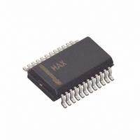
MAX1168BCEG+ Maxim Integrated Products, MAX1168BCEG+ Datasheet - Page 23

MAX1168BCEG+
Manufacturer Part Number
MAX1168BCEG+
Description
IC ADC 16BIT 200KSPS 24-QSOP
Manufacturer
Maxim Integrated Products
Datasheet
1.MAX1167BEEE.pdf
(30 pages)
Specifications of MAX1168BCEG+
Number Of Bits
16
Sampling Rate (per Second)
200k
Data Interface
MICROWIRE™, QSPI™, Serial, SPI™
Number Of Converters
1
Power Dissipation (max)
762mW
Voltage Supply Source
Analog and Digital
Operating Temperature
0°C ~ 70°C
Mounting Type
Surface Mount
Package / Case
24-QSOP
Lead Free Status / RoHS Status
Lead free / RoHS Compliant
The input data latches on the falling edge of SCLK. The
command/configuration/control register starts reading
data in on the falling edge of the first SCLK cycle immedi-
ately following the falling edge of the frame sync pulse
and ends on the falling edge of the 16th SCLK cycle. The
MAX1168 selects the proper channel for conversion on
the falling edge of the 3rd clock cycle and begins acqui-
sition. Acquisition continues until the rising edge of the
15th clock cycle. The MAX1168 samples the input on the
rising edge of the 15th clock cycle. On the rising edge of
the 16th clock cycle, the MAX1168 outputs a frame sync
pulse at DSPX. The frame sync pulse alerts the DSP that
the conversion results are about to be output at DOUT
(MSB first) starting on the rising edge of the 17th clock
pulse. To read the entire conversion result, 16 SCLK
cycles are needed. Extra clock pulses, occurring after the
conversion result has been clocked out and prior to the
next rising edge of DSPR, cause zeros to be clocked out
of DOUT. The MAX1168 external clock, DSP 16-bit-wide
data-transfer mode requires 32 clock cycles to complete.
Figure 20a. SPI Connections
Figure 20c. SPI/MICROWIRE Interface Timing Sequence (CPOL = CPHA = 0)
DOUT*
SCLK
Multichannel, 16-Bit, 200ksps Analog-to-Digital
CS
*WHEN CS IS HIGH, DOUT = HIGH-Z
SPI
0
1
MISO
SCK
I/O
SS
______________________________________________________________________________________
0
0
V
DD
1ST BYTE READ
0
4
0
CS
SCLK
DOUT
D7
MAX1167
MAX1168
0
6
D6
0
0
D5
8
3RD BYTE READ
D4
20
D3
Begin a new conversion by sending a new frame sync
pulse to DSPR followed by new configuration data.
Send the new DSPR pulse immediately after reading
the conversion result to realize maximum throughput.
Sending a new frame sync pulse in the middle of a con-
version immediately aborts the current conversion and
begins a new one. A rising edge on CS in the middle of
a conversion aborts the current conversion and places
the MAX1168 in shutdown.
The data output from the MAX1167/MAX1168 is straight
binary. Figure 19 shows the nominal transfer function.
Code transitions occur halfway between successive
integer LSB values (V
+62.5µV or 4.096V / 65,536V).
Figure 20b. MICROWIRE Connections
D2
MSB
D15
Output Coding and Transfer Function
D1
MICROWIRE
LSB
D14
D0
24
I/O
SK
SI
D13
HIGH-Z
2ND BYTE READ
D12
REF
12
D11
= +4.096V, and 1 LSB =
Converters
D10
CS
SCLK
DOUT
MAX1168
MAX1167
D9
D8
16
D7
23


