MAX1168BCEG+ Maxim Integrated Products, MAX1168BCEG+ Datasheet - Page 26

MAX1168BCEG+
Manufacturer Part Number
MAX1168BCEG+
Description
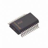
IC ADC 16BIT 200KSPS 24-QSOP
Manufacturer
Maxim Integrated Products
Datasheet
1.MAX1167BEEE.pdf
(30 pages)
Specifications of MAX1168BCEG+
Number Of Bits
16
Sampling Rate (per Second)
200k
Data Interface
MICROWIRE™, QSPI™, Serial, SPI™
Number Of Converters
1
Power Dissipation (max)
762mW
Voltage Supply Source
Analog and Digital
Operating Temperature
0°C ~ 70°C
Mounting Type
Surface Mount
Package / Case
24-QSOP
Lead Free Status / RoHS Status
Lead free / RoHS Compliant
Multichannel, 16-Bit, 200ksps Analog-to-Digital
Converters
Figure 22b. SPI Interface Timing with PIC16/PIC17 in Master Mode (CKE = 1, CKP = 0, SMP = 0, SSPM3 - SSPM0 = 0001)
Figure 23. DSP Interface Connection
When using the SPI (Figure 20a) or MICROWIRE (Figure
20b) interfaces, set CPOL = 0 and CPHA = 0. Drive CS
low to power on the MAX1167/MAX1168 before starting a
conversion (Figure 20c). Three consecutive 8-bit-wide
readings are necessary to obtain the entire 16-bit result
from the ADC. DOUT data transitions on the serial clock’s
falling edge. The first 8-bit-wide data stream contains all
leading zeros. The 2nd 8-bit-wide data stream contains
the MSB through D6. The 3rd 8-bit-wide data stream con-
tains D5 through D0 followed by S1 and S0.
26
DOUT*
SCLK
CS
______________________________________________________________________________________
*WHEN CS IS HIGH, DOUT = HIGH-Z
0
DSP
1
SCLK
RFS
TFS
FL1
0
DR
DT
SPI and MICROWIRE Interfaces
0
EXTERNAL
CLOCK
1ST BYTE READ
0
4
0
SCLK
DSPR
DSPX
DIN
DOUT
CS
Serial Interfaces
D7
0
MAX1168
6
D6
0
0
D5
8
3RD BYTE READ
D4
20
D3
Using the high-speed QSPI interface with CPOL = 0 and
CPHA = 0, the MAX1167/MAX1168 support a maximum
f
MAX1168 connected to a QSPI master, and Figure 21b
shows the associated interface timing.
The MAX1167/MAX1168 are compatible with a
PIC16/PIC17 controller (µC), using the synchronous seri-
al-port (SSP) module.
To establish SPI communication, connect the controller
as shown in Figure 22a and configure the PIC16/PIC17
as system master by initializing its synchronous serial-
port control register (SSPCON) and synchronous serial-
port status register (SSPSTAT) to the bit patterns shown
in Tables 7 and 8.
In SPI mode, the PIC16/PIC17 µCs allow 8 bits of data to
be synchronously transmitted and received simultane-
ously. Three consecutive 8-bit-wide readings (Figure
22b) are necessary to obtain the entire 16-bit result from
the ADC. DOUT data transitions on the serial clock’s
falling edge and is clocked into the µC on SCLK’s rising
edge. The first 8-bit-wide data stream contains all zeros.
The 2nd 8-bit-wide data stream contains the MSB
through D6. The 3rd 8-bit-wide data stream contains bits
D5 through D0 followed by S1 and S0.
SCLK
D2
MSB
D15
of 4.8MHz. Figure 21a shows the MAX1167/
D1
PIC16 with SSP Module and PIC17
D0
D14
LSB
24
D13
HIGH-Z
D12
2ND BYTE READ
12
D11
D10
D9
QSPI Interface
D8
16
Interface


