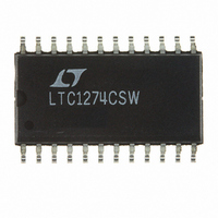
LTC1274CSW Linear Technology, LTC1274CSW Datasheet - Page 10

LTC1274CSW
Manufacturer Part Number
LTC1274CSW
Description
IC A/D CONV 12BIT W/SHTDN 24SOIC
Manufacturer
Linear Technology
Datasheet
1.LTC1274CSWPBF.pdf
(20 pages)
Specifications of LTC1274CSW
Number Of Bits
12
Sampling Rate (per Second)
100k
Data Interface
Parallel
Number Of Converters
1
Power Dissipation (max)
20mW
Voltage Supply Source
Dual ±
Operating Temperature
0°C ~ 70°C
Mounting Type
Surface Mount
Package / Case
24-SOIC (0.300", 7.50mm Width)
Lead Free Status / RoHS Status
Contains lead / RoHS non-compliant
Other names
LTC1274CS
Available stocks
Company
Part Number
Manufacturer
Quantity
Price
Part Number:
LTC1274CSW
Manufacturer:
LT/凌特
Quantity:
20 000
Company:
Part Number:
LTC1274CSW#PBF
Manufacturer:
LT
Quantity:
4 420
Company:
Part Number:
LTC1274CSW#TRPBF
Manufacturer:
ON
Quantity:
5 600
APPLICATIONS
CONVERSION DETAILS
The LTC1274/LTC1277 use a successive approximation
algorithm and an internal sample-and-hold circuit to con-
vert an analog signal to a 12-bit parallel output. The ADCs
are complete with a precision reference and an internal
clock. The control logic provides easy interface to micro-
processors and DSPs. (Please refer to the Digital Interface
section for the data format.)
Conversion start is controlled by the CS and CONVST
inputs. At the start of conversion the successive approxi-
mation register (SAR) is reset. Once a conversion cycle
has begun it cannot be restarted.
During conversion, the internal 12-bit capacitive DAC out-
put is sequenced by the SAR from the most significant bit
(MSB) to the least significant bit (LSB). Referring to
Figure 1, the A
nects to the sample-and-hold capacitor during the acquire
phase, and the comparator offset is nulled by the feedback
switch. In this acquire phase, a minimum delay of 2µs will
provide enough time for the sample-and-hold capacitor to
acquire the analog signal. During the convert phase, the
comparator feedback switch opens, putting the comparator
into the compare mode. The input switch connects C
to ground (LTC1274) or A
analog input charge onto the summing junction. This input
charge is successively compared with the binary-weighted
LTC1274/LTC1277
TI I G DIAGRA S
10
W
U
NAP to CONVST Wake-Up Timing (LTC1277)
CONVST
RD
CS
NAP
IN
(LTC1274) or A
CS to RD Setup Timing
U
t
1
INFORMATION
t
U
3
W
IN
–
(LTC1277), injecting the
IN
+
LTC1274/77 • TD01
(LTC1277) input con-
W
LTC1274/77 • TD03
U
SAMPLE
charges supplied by the capacitive DAC. Bit decisions are
made by the high speed comparator. At the end of a
conversion, the DAC output balances the A
A
bit data word) which represent the A
A
DYNAMIC PERFORMANCE
The LTC1274/LTC1277 have excellent high speed sam-
pling capability. FFT (Fast Fourier Transform) test tech-
niques are used to test the ADCs’ frequency response,
distortion and noise at the rated throughput. By applying
a low distortion sine wave and analyzing the digital output
IN
IN
+
+
A
– A
– A
IN
IN
IN
SAMPLE
–
HOLD
–
CONVST
(LTC1277) are loaded into the 12-bit output latches.
(LTC1277) input charge. The SAR contents (a 12-
REFRDY
CS
SLEEP to REFRDY Wake-Up Timing
SLEEP
C
CS to CONVST Setup Timing
Figure 1. LTC1274 A
SAMPLE
C
V
DAC
DAC
t
14
t
2
DAC
IN
SAMPLE
–
+
LTC1274/77 • TD02
COMPAR-
Input
ATOR
LTC1274/77 • TD04
SI
IN
IN
(LTC1274) or
(LTC1274) or
LATCH
1274 • F01
12-BIT
S
A
R


