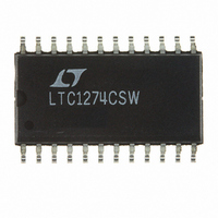
LTC1274CSW Linear Technology, LTC1274CSW Datasheet - Page 16

LTC1274CSW
Manufacturer Part Number
LTC1274CSW
Description
IC A/D CONV 12BIT W/SHTDN 24SOIC
Manufacturer
Linear Technology
Datasheet
1.LTC1274CSWPBF.pdf
(20 pages)
Specifications of LTC1274CSW
Number Of Bits
12
Sampling Rate (per Second)
100k
Data Interface
Parallel
Number Of Converters
1
Power Dissipation (max)
20mW
Voltage Supply Source
Dual ±
Operating Temperature
0°C ~ 70°C
Mounting Type
Surface Mount
Package / Case
24-SOIC (0.300", 7.50mm Width)
Lead Free Status / RoHS Status
Contains lead / RoHS non-compliant
Other names
LTC1274CS
Available stocks
Company
Part Number
Manufacturer
Quantity
Price
Part Number:
LTC1274CSW
Manufacturer:
LT/凌特
Quantity:
20 000
Company:
Part Number:
LTC1274CSW#PBF
Manufacturer:
LT
Quantity:
4 420
Company:
Part Number:
LTC1274CSW#TRPBF
Manufacturer:
ON
Quantity:
5 600
LTC1274/LTC1277
A
adjusted before full-scale error. Bipolar offset error ad-
justment is achieved by trimming the offset adjust while
the input voltage is 0.5LSB below ground. This is done by
applying an input voltage of – 0.50mV (– 0.5LSB) to the
input in Figure 11c and adjusting the R8 until the ADC’s
output code flickers between 0000 0000 0000 and 1111
1111 1111 in LTC1274 or between 0111 1111 1111 and
1000 0000 0000 in LTC1277. For full-scale adjustment, an
input voltage of 2.0465V (FS – 1.5LSBs) is applied to the
input and R5 is adjusted until the output code flickers
between 0111 1111 1110 and 0111 1111 1111 in LTC1274
or between 1111 1111 1110 and 1111 1111 1111 in
LTC1277.
Internal Clock
The A/D converters have an internal clock that eliminates
the need of synchronization between the external clock
and the CS and RD signals found in other ADCs. The
internal clock is factory trimmed to achieve a typical
conversion time of 6µs. No external adjustments are
required and with the maximum acquisition time of 2µs
throughput performance of 100ksps is assured.
Timing and Control
Conversion start and data read operations are controlled
by three digital inputs in the LTC1274: CS, CONVST and
RD. For the LTC1277 there are four digital inputs: CS,
CONVST, RD and HBEN. Figure 12 shows the logic
structure associated with these inputs for LTC1277. A
falling edge on CONVST will start a conversion after the
ADC has been selected (i.e., CS is low). Once initiated, it
cannot be restarted until the conversion is complete.
Converter status is indicated by the BUSY output and this
is low while conversion is in progress. The High Byte
Enable input (HBEN) in the LTC1277 is to multiplex the 12
bits of conversion data onto the lower D7 to D0/8
outputs.
Figures 13 through 17 show several different modes of
operation. In modes 1a and 1b (Figures 13 and 17) CS and
RD are both tied low. The falling edge of CONVST starts the
conversion. The data outputs are always enabled and data
can be latched with the BUSY rising edge. Mode 1a shows
operation with a narrow logic low CONVST pulse. Mode 1b
shows a narrow logic high CONVST pulse.
16
PPLICATI
O
U
S
I FOR ATIO
U
W
U
ANALOG
ANALOG
4.096V
V1
INPUT
INPUT
0V TO
5V
50Ω
R1
Figure 11b. LTC1274/LTC1277 Unipolar Offset and
Full-Scale Adjust Circuit
10k
R1
Figure 11c. LTC1274/LTC1277 Bipolar Offset and
Full-Scale Adjust Circuit
10k
10k
R1
20Ω
10k
R9
R2
ADDITIONAL PINS OMITTED FOR CLARITY
±20LSB TRIM RANGE
Figure 11a. Full-Scale Adjust Circuit
R2
10k
R2
10k
+
–
+
–
R3
10k
+
–
400Ω
100k
A1
200Ω
100k
R3
R6
R3
R6
FULL-SCALE
ADJUST
100Ω
R4
100k
R5
4.3k
FULL-SCALE
ADJUST
R4
100k
R4
100k
R5
4.3k
FULL-SCALE
ADJUST
R7
100k
R7
–5V
5V
5V
R8
10k
OFFSET
ADJUST
R8
20k
OFFSET
ADJUST
A
A
AGND
A
IN
IN
IN
A
A
A
+
LTC1274
LTC1277
–
A
A
A
(LTC1274)
IN
IN
IN
IN
IN
IN
(LTC1277)
(LTC1277)
+
LTC1274
LTC1277
–
LTC1274/77 F11a
(LTC1274)
+
LTC1274
LTC1277
–
(LTC1274)
(LTC1277)
(LTC1277)
(LTC1277)
(LTC1277)
LTC1274/77 F11b
LTC1274/77 F11c


