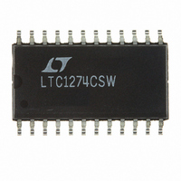
LTC1274CSW Linear Technology, LTC1274CSW Datasheet - Page 14

LTC1274CSW
Manufacturer Part Number
LTC1274CSW
Description
IC A/D CONV 12BIT W/SHTDN 24SOIC
Manufacturer
Linear Technology
Datasheet
1.LTC1274CSWPBF.pdf
(20 pages)
Specifications of LTC1274CSW
Number Of Bits
12
Sampling Rate (per Second)
100k
Data Interface
Parallel
Number Of Converters
1
Power Dissipation (max)
20mW
Voltage Supply Source
Dual ±
Operating Temperature
0°C ~ 70°C
Mounting Type
Surface Mount
Package / Case
24-SOIC (0.300", 7.50mm Width)
Lead Free Status / RoHS Status
Contains lead / RoHS non-compliant
Other names
LTC1274CS
Available stocks
Company
Part Number
Manufacturer
Quantity
Price
Part Number:
LTC1274CSW
Manufacturer:
LT/凌特
Quantity:
20 000
Company:
Part Number:
LTC1274CSW#PBF
Manufacturer:
LT
Quantity:
4 420
Company:
Part Number:
LTC1274CSW#TRPBF
Manufacturer:
ON
Quantity:
5 600
LTC1274/LTC1277
A
Figure 8. For bipolar mode, a 0.1µF ceramic provides
adequate bypassing for the V
be located as close to the pins as possible. The traces
connecting the pins and bypass capacitors must be kept
short and should be made as wide as possible.
Input signal leads to A
AGND (Pin 3 for LTC1274, Pin 4 for LTC1277) should be
kept as short as possible to minimize input noise cou-
pling. In applications where this is not possible a shielded
cable between source and ADC is recommended.
Also, since any potential difference in grounds between
the signal source and the ADC appears as an error voltage
in series with the input signal, attention should be paid to
reducing the ground circuit impedances as much as
possible.
A single point analog ground separate from the logic
system ground should be established with an analog
14
PPLICATI
O
V
U
REF
S
OUTPUT
IN
2.42V
CIRCUITRY
I FOR ATIO
ANALOG
and signal return leads from
U
INPUT
10µF
SS
+
pin. The capacitors must
1
+
–
W
ANALOG INPUT
A
(0V TO 4.095V)
PARALLEL
IN
12-BIT
0.1µF
Figure 8. Power Supply Grounding Practice
AGND
BUS
3
Figure 9. LTC1274 Typical Circuit
ANALOG GROUND PLANE
10
11
12
10µF
U
1
2
3
4
5
6
7
8
9
A
V
AGND
D11 (MSB)
D10
D9
D8
D7
D6
D5
D4
DGND
IN
REF
V
REF
LTC1274
2
0.1µF
CONVST
REFRDY
LTC1274
SLEEP
BUSY
V
V
RD
ground plane at AGND or as close as possible to the ADC.
DGND (Pin 12) and all other analog grounds should be
connected to this single analog ground point. No other
digital grounds should be connected to this analog ground
point. Low impedance analog and digital power supply
common returns are essential to low noise operation of
the ADC and the foil width for these tracks should be as
wide as possible. In applications where the ADC data
outputs and control signals are connected to a continu-
ously active microprocessor bus, it is possible to get
errors in conversion results. These errors are due to
feedthrough from the microprocessor to the successive
approximation comparator. The problem can be elimi-
nated by forcing the microprocessor into a Wait state
during conversion or by using three-state buffers to
isolate the ADC data bus. Figure 9 is a typical application
circuit for the LTC1274.
DD
CS
D0
D1
D2
D3
SS
10µF
24
23
22
21
20
19
18
17
16
15
14
13
AV
µP
CONTROL
LINES
DD
CONVERSION START INPUT
SLEEP MODE INPUT
REFERENCE READY SIGNAL
24
0.1µF
DV
10µF
DD
LTC1274/77 • F09
17
+
DGND
12
5V
GROUND CONNECTION
TO DIGITAL CIRCUITRY
0.1µF
DIGITAL
SYSTEM
LTC1274/77 • F08


