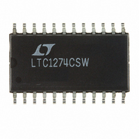
LTC1274CSW Linear Technology, LTC1274CSW Datasheet - Page 15

LTC1274CSW
Manufacturer Part Number
LTC1274CSW
Description
IC A/D CONV 12BIT W/SHTDN 24SOIC
Manufacturer
Linear Technology
Datasheet
1.LTC1274CSWPBF.pdf
(20 pages)
Specifications of LTC1274CSW
Number Of Bits
12
Sampling Rate (per Second)
100k
Data Interface
Parallel
Number Of Converters
1
Power Dissipation (max)
20mW
Voltage Supply Source
Dual ±
Operating Temperature
0°C ~ 70°C
Mounting Type
Surface Mount
Package / Case
24-SOIC (0.300", 7.50mm Width)
Lead Free Status / RoHS Status
Contains lead / RoHS non-compliant
Other names
LTC1274CS
Available stocks
Company
Part Number
Manufacturer
Quantity
Price
Part Number:
LTC1274CSW
Manufacturer:
LT/凌特
Quantity:
20 000
Company:
Part Number:
LTC1274CSW#PBF
Manufacturer:
LT
Quantity:
4 420
Company:
Part Number:
LTC1274CSW#TRPBF
Manufacturer:
ON
Quantity:
5 600
A
DIGITAL INTERFACE
The ADCs are designed to interface with microproces-
sors as a memory mapped device. The CS and RD control
inputs are common to all peripheral memory interfacing.
A separate CONVST is used to initiate a conversion.
Figures 10a to 10c are the input/output characteristics of
the ADCs. The code transitions occur midway between
successive integer LSB values (i.e., 0.5LSB, 1.5LSB,
2.5LSB…FS – 1.5LSV). The output code is scaled such
that 1.0LSB = FS/4096 = 4.096V/4096 = 1.0mV.
Unipolar Offset and Full-Scale Error Adjustments
In applications where absolute accuracy is important, then
offset and full-scale errors can be adjusted to zero. Offset
PPLICATI
111...111
111...110
111...101
111...100
000...011
000...010
000...001
000...000
Figure 10a. LTC1274/LTC1277 Unipolar
Transfer Characteristics
0V
UNIPOLAR
ZERO
1LSB = FS
LSB
O
1
U
4096
S
INPUT VOLTAGE (V)
=
I FOR ATIO
4.096V
U
4096
= 1mV
Figure 10c. LTC1277 Bipolar Transfer Characteristics
(Offset Binary)
111...111
111...110
100...001
100...000
011...111
011...110
000...001
000...000
W
LTC1274/77 F10a
FS – 1LSB
–FS/2
U
INPUT VOLTAGE (V)
1LSB =
BIPOLAR
LSB
–1
ZERO
4096
FS
0V
LSB
=
error must be adjusted before full-scale error. Figure 11a
shows the extra components required for full-scale error
adjustment. If both offset and full-scale adjustments are
needed, the circuit in Figure 11b can be used. For zero
offset error, apply 0.50mV (i.e., 0.5LSB) at the input and
adjust the offset trim until the LTC1274/LTC1277 output
code flickers between 0000 0000 0000 and 0000 0000
0001. For zero full-scale error, apply an analog input of
4.0945V (i.e., FS – 1.5LSB or last code transition) at the
input and adjust R5 until the ADC output code flickers
between 1111 1111 1110 and 1111 1111 1111.
Bipolar Offset and Full-Scale Error Adjustments
Bipolar offset and full-scale errors are adjusted in a similar
fashion to the unipolar case. Again, bipolar offset must be
1
4.096V
4096
LTC1274/77 • F10c
FS/2 – 1LSB
= 1mV
011...111
011...110
000...001
000...000
111...111
111...110
100...001
100...000
Figure 10b. LTC1274 Bipolar Transfer
Characteristics (2’s Complement)
–FS/2
INPUT VOLTAGE (V)
LTC1274/LTC1277
1LSB =
BIPOLAR
LSB
–1
ZERO
4096
FS
0V
LSB
=
1
4.096V
4096
LTC1274/77 • F10b
FS/2 – 1LSB
= 1mV
15


