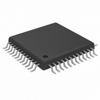
MAX1183ECM+TD Maxim Integrated Products, MAX1183ECM+TD Datasheet - Page 12

MAX1183ECM+TD
Manufacturer Part Number
MAX1183ECM+TD
Description
IC ADC 10BIT 40MSPS DL 48-TQFP
Manufacturer
Maxim Integrated Products
Datasheet
1.MAX1183ECMD.pdf
(18 pages)
Specifications of MAX1183ECM+TD
Number Of Bits
10
Sampling Rate (per Second)
40M
Data Interface
Parallel
Number Of Converters
2
Power Dissipation (max)
180mW
Voltage Supply Source
Single Supply
Operating Temperature
-40°C ~ 85°C
Mounting Type
Surface Mount
Package / Case
48-TQFP Exposed Pad, 48-eTQFP, 48-HTQFP, 48-VQFP
Lead Free Status / RoHS Status
Lead free / RoHS Compliant
where f
t
Clock jitter is especially critical for undersampling
applications. The clock input should always be consid-
ered as an analog input and routed away from any ana-
log input or other digital signal lines.
The MAX1183 clock input operates with a voltage thresh-
old set to V
than 50% must meet the specifications for high and low
periods as stated in the Electrical Characteristics.
Figure 3 depicts the relationship between the clock
input, analog input, and data output. The MAX1183
samples at the rising edge of the input clock. Output
data for channels A and B is valid on the next rising
edge of the input clock. The output data has an internal
latency of five clock cycles. Figure 4 also determines
the relationship between the input clock parameters
and the valid output data on channels A and B.
Dual 10-Bit, 40Msps, 3V, Low-Power ADC with
Internal Reference and Parallel Outputs
Figure 3. System Timing Diagram
12
AJ
ANALOG INPUT
is the time of the aperture jitter.
DATA OUTPUT
DATA OUTPUT
CLOCK INPUT
______________________________________________________________________________________
D9A–D0A
D9B–D0B
IN
represents the analog input frequency and
DD
/2. Clock inputs with a duty cycle other
System Timing Requirements
t
DO
N - 6
N - 6
N
N - 5
N - 5
N + 1
N - 4
N - 4
5-CLOCK-CYCLE LATENCY
N + 2
t
CH
All digital outputs, D0A–D9A (Channel A) and D0B–D9B
(Channel B) are TTL/CMOS logic-compatible. There is a
five-clock-cycle latency between any particular sample
and its corresponding output data. The output coding
can be chosen to be either straight offset binary or
two’s complement (Table 1) controlled by a single pin
(T/B). Pull T/B low to select offset binary and high to
activate two’s complement output coding. The capaci-
tive load on the digital outputs D0A–D9A and D0B–D9B
should be kept as low as possible (<15pF) to avoid
large digital currents that could feed back into the ana-
log portion of the MAX1183, thereby degrading its
dynamic performance. Using buffers on the digital out-
puts of the ADCs can further isolate the digital outputs
from heavy capacitive loads. To further improve the
dynamic performance of the MAX1183, small-series
resistors (e.g., 100Ω) may be added to the digital out-
put paths close to the MAX1183.
N - 3
N - 3
Digital Output Data, Output Data Format
N + 3
Selection (T/B), Output Enable ( OE )
N - 2
N - 2
t
CL
N + 4
N - 1
N - 1
N + 5
N
N
N + 6
N + 1
N + 1


