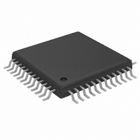
MAX1183ECM+TD Maxim Integrated Products, MAX1183ECM+TD Datasheet - Page 5

MAX1183ECM+TD
Manufacturer Part Number
MAX1183ECM+TD
Description
IC ADC 10BIT 40MSPS DL 48-TQFP
Manufacturer
Maxim Integrated Products
Datasheet
1.MAX1183ECMD.pdf
(18 pages)
Specifications of MAX1183ECM+TD
Number Of Bits
10
Sampling Rate (per Second)
40M
Data Interface
Parallel
Number Of Converters
2
Power Dissipation (max)
180mW
Voltage Supply Source
Single Supply
Operating Temperature
-40°C ~ 85°C
Mounting Type
Surface Mount
Package / Case
48-TQFP Exposed Pad, 48-eTQFP, 48-HTQFP, 48-VQFP
Lead Free Status / RoHS Status
Lead free / RoHS Compliant
ELECTRICAL CHARACTERISTICS (continued)
(V
10kΩ resistor, V
unless otherwise noted. Typical values are at T
(V
otherwise noted.)
Note 1: Equivalent dynamic performance is obtainable over full OV
Note 2: Specifications at ≥ +25°C are guaranteed by production test and < +25°C are guaranteed by design and characterization.
Note 3: SNR, SINAD, THD, SFDR, and HD3 are based on an analog input voltage of -0.5dBFS referenced to a 1.024V full-scale
Note 4: Intermodulation distortion is the total power of the intermodulation products relative to the individual carrier. This number is
Note 5: Digital outputs settle to V
Note 6: With REFIN driven externally, REFP, COM, and REFN are left floating while powered down.
CHANNEL-TO-CHANNEL MATCHING
CLK Pulse Width High
CLK Pulse Width Low
Wake-Up Time
Crosstalk
Gain Matching
Phase Matching
DD
DD
-100
-10
-20
-30
-40
-50
-60
-70
-80
-90
= 3V, OV
0
Dual 10-Bit, 40Msps, 3V, Low-Power ADC with
= 3V, OV
0
input voltage range.
6dB better, if referenced to the two-tone envelope.
FFT PLOT CHA (DIFFERENTIAL INPUT,
PARAMETER
2
8192-POINT DATA RECORD)
ANALOG INPUT FREQUENCY (MHz)
CHA
4
DD
DD
IN
6
= 2.5V, 0.1µF and 1.0µF capacitors from REFP, REFN, and COM to GND, REFOUT connected to REFIN through a
= 2V
= 2.5V, V
_______________________________________________________________________________________
8
Internal Reference and Parallel Outputs
P-P
10 12 14
f
f
f
A
CLK
INA
INB
INA
(differential with respect to COM), C
= 7.5343MHz
= 6.1475MHz
= 40.0006MHz
= -0.498dBFS
HD2
REFIN
HD3
IH
16
, V
= 2.048V, differential input at -0.5dBFS, f
SYMBOL
18
IL
t
WAKE
t
. Parameter guaranteed by design.
t
CH
20
CL
A
-100
= +25°C.) (Note 2)
Figure 3, clock period: 25ns
Figure 3, clock period: 25ns
Wake up from sleep mode (Note 6)
Wake up from shutdown (Note 6)
f
f
f
-10
-20
-30
-40
-50
-60
-70
-80
-90
INA or B
INA or B
INA or B
0
0
FFT PLOT CHB (DIFFERENTIAL INPUT,
2
CHB
= 20MHz at -0.5dBFS
= 20MHz at -0.5dBFS
= 20MHz at -0.5dBFS
8192-POINT DATA RECORD)
ANALOG INPUT FREQUENCY (MHz)
4
L
6
= 10pF at digital outputs (Note 1), f
CONDITIONS
8
DD
HD2
10 12 14
f
f
f
A
range with reduced C
CLK
INB
INA
Typical Operating Characteristics
INB
= 6.1475MHz
= 7.5343MHz
= 40.0006MHz
= -0.534dBFS
HD3
CLK
16
18
= 40.0006MHz, C
20
L
.
-100
-10
-20
-30
-40
-50
-60
-70
-80
-90
0
MIN
0
FFT PLOT CHA (DIFFERENTIAL INPUT,
CLK
f
f
f
A
CLK
INA
INB
INA
HD3
2
L
= 24.9662MHz
= 19.888MHz
= 40.0006MHz
= -0.552dBFS
8192-POINT DATA RECORD)
ANALOG INPUT FREQUENCY (MHz)
≈ 10pF, T
= 40MHz, T
4
±3.8
±3.8
TYP
12.5
12.5
0.41
0.02
0.25
-70
6
1.5
HD2
8
A
10 12 14
A
= +25°C, unless
MAX
±0.2
= T
MIN
16
Degrees
to T
UNITS
CHA
dB
dB
18
ns
ns
µs
MAX
20
5
,


