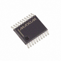
MAX1301BEUP+ Maxim Integrated Products, MAX1301BEUP+ Datasheet - Page 12

MAX1301BEUP+
Manufacturer Part Number
MAX1301BEUP+
Description
IC ADC 16BIT SER 4CH LP 20TSSOP
Manufacturer
Maxim Integrated Products
Datasheet
1.MAX1301BEUPT.pdf
(32 pages)
Specifications of MAX1301BEUP+
Number Of Bits
16
Sampling Rate (per Second)
115k
Data Interface
MICROWIRE™, QSPI™, Serial, SPI™
Number Of Converters
1
Power Dissipation (max)
105.5mW
Voltage Supply Source
Analog and Digital
Operating Temperature
-40°C ~ 85°C
Mounting Type
Surface Mount
Package / Case
20-TSSOP
Lead Free Status / RoHS Status
Lead free / RoHS Compliant
8- and 4-Channel, ±3 x V
Serial 16-Bit ADCs
12
MAX1300 MAX1301
10
11
12
13
14
15
16
17
18
19
20
1
2
3
4
5
6
7
8
9
______________________________________________________________________________________
PIN
10
11
12
13
14
15
16
17
—
—
—
—
2
3
4
5
6
7
8
9
REFCAP
DGNDO Digital I/O Ground. DGND, DGNDO, AGND3, AGND2, and AGND1 must be connected together.
DV
SSTRB
AV
NAME
DGND
DOUT
SCLK
DV
CH0
CH1
CH2
CH3
CH4
CH5
CH6
CH7
REF
DIN
CS
DDO
DD1
DD
Analog Supply Voltage 1. Connect AV
AV
Analog Input Channel 0
Analog Input Channel 1
Analog Input Channel 2
Analog Input Channel 3
Analog Input Channel 4
Analog Input Channel 5
Analog Input Channel 6
Analog Input Channel 7
Active-Low Chip-Select Input. When CS is low, data is clocked into the device from DIN on the
rising edge of SCLK. With CS low, data is clocked out of DOUT on the falling edge of SCLK.
When CS is high, activity on SCLK and DIN is ignored and DOUT is high impedance.
Serial Data Input. When CS is low, data is clocked in on the rising edge of SCLK. When CS is
high, transitions on DIN are ignored.
Serial-Strobe Output. When using the internal clock, SSTRB rising edge transitions indicate that
data is ready to be read from the device. When operating in external clock mode, SSTRB is
always low. SSTRB does not tri-state, regardless of the state of CS, and therefore requires
a dedicated I/O line.
Serial Clock Input. When CS is low, transitions on SCLK clock data into DIN and out of DOUT.
When CS is high, transitions on SCLK are ignored.
Serial Data Output. When CS is low, data is clocked out of DOUT with each falling SCLK
transition. When CS is high, DOUT is high impedance.
Digital Ground. DGND, DGNDO, AGND3, AGND2, and AGND1 must be connected together.
Digital I/O Supply Voltage Input. Connect DV
Bypass DV
Digital-Supply Voltage Input. Connect DV
Bypass DV
Bandgap-Voltage Bypass Node. For external reference operation, connect REFCAP to AV
For internal reference operation, bypass REFCAP with a 0.01μF capacitor to AGND1
(V
Reference-Buffer Output/ADC Reference Input. For external reference operation, apply an
external reference voltage from 3.800V to 4.136V to REF. For internal reference operation,
bypassing REF with a 1μF capacitor to AGND1 sets V
REFCAP
DD1
to AGND1 with a 0.1μF capacitor.
≈ 4.096V).
DDO
DD
to DGND with a 0.1μF capacitor.
to DGNDO with a 0.1μF capacitor.
REF
DD1
DD
to a +4.75V to +5.25V power-supply voltage. Bypass
FUNCTION
Multirange Inputs,
to a +4.75V to +5.25V power-supply voltage.
DDO
to a +2.7V to +5.25V power-supply voltage.
REF
= 4.096V ±1%.
Pin Description
DD
.


