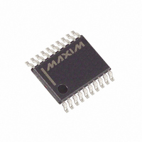
MAX1301BEUP+ Maxim Integrated Products, MAX1301BEUP+ Datasheet - Page 6

MAX1301BEUP+
Manufacturer Part Number
MAX1301BEUP+
Description
IC ADC 16BIT SER 4CH LP 20TSSOP
Manufacturer
Maxim Integrated Products
Datasheet
1.MAX1301BEUPT.pdf
(32 pages)
Specifications of MAX1301BEUP+
Number Of Bits
16
Sampling Rate (per Second)
115k
Data Interface
MICROWIRE™, QSPI™, Serial, SPI™
Number Of Converters
1
Power Dissipation (max)
105.5mW
Voltage Supply Source
Analog and Digital
Operating Temperature
-40°C ~ 85°C
Mounting Type
Surface Mount
Package / Case
20-TSSOP
Lead Free Status / RoHS Status
Lead free / RoHS Compliant
ELECTRICAL CHARACTERISTICS (continued)
(AV
external clock mode, V
(±3 x V
8- and 4-Channel, ±3 x V
Serial 16-Bit ADCs
Note 1: Parameter tested at AV
Note 2: See definitions in the Parameter Definitions section at the end of the data sheet.
Note 3: Guaranteed by correlation with single-ended measurements.
Note 4: Not production tested. Guaranteed by design.
Note 5: To ensure external reference operation, V
Note 6: The SCLK duty cycle can vary between 40% and 60%, as long as the t
(AV
external clock mode, V
C
6
SCLK Fall to
SSTRB Rise to
DOUT Rise/Fall Time
SSTRB Rise/Fall Time
DOUT
DD1
DD1
2.6
2.5
2.4
2.3
2.2
2.1
_______________________________________________________________________________________
Rise to DOUT Disable
Fall to SCLK Rise Setup
High Minimum Pulse Width
4.75
REF
= 50pF, C
= AV
= AV
must be below (AV
sition point between internal reference mode and external reference mode lies between the REFCAP buffer disable threshold
minimum and maximum values (Figures 17 and 18).
EXTERNAL CLOCK MODE
T
), C
PARAMETER
A
vs. ANALOG SUPPLY VOLTAGE
= -40°C
ANALOG SUPPLY CURRENT
4.85
DD2
DD2
DOUT
= DV
= DV
Rise Hold
SSTRB
4.95
= 50pF, C
Fall Setup
V
T
AVDD1
A
DD
= +25°C
DD
REF
REF
= 50pF; unless otherwise noted.)
(V)
= DV
5.05
= DV
DD1
= 4.096V (external reference operation), REFCAP = AV
= 4.096V (external reference operation), REFCAP = AV
SSTRB
T
- 0.4V). Bypassing REFCAP with a 0.1μF or larger capacitor to AGND1 sets V REFCAP ≈ 4.096V. The tran-
DDO
A
DDO
DD1
= +85°C
5.15
= 5V, AGND1 = DGND = DGNDO = AGND2 = AGND3 = 0, f
= 50pF, T
= AV
= 5V, AGND1 = DGND = DGNDO = AGND2 = AGND3 = 0, f
SYMBOL
t
5.25
CSPW
t
t
CSH
t
CSS
TR
DD2
= DV
A
= -40°C to +85°C, unless otherwise noted. Typical values are at T
REFCAP
(Note 4)
C
C
18
17
16
15
14
13
12
11
10
DD
L
L
4.75
= 50pF
= 50pF
vs. PREAMPLIFIER SUPPLY VOLTAGE
= DV
PREAMPLIFIER SUPPLY CURRENT
must exceed (AV
4.85
DDO
CONDITIONS
= 5V.
4.95
V
AVDD2
REF
EXTERNAL CLOCK MODE
T
T
T
A
A
A
= +85°C
= +25°C
= -40°C
AIN1–AIN7 = AGND2
Typical Operating Characteristics
(V)
5.05
DD1
AIN0 = +FS
5.15
- 0.1V). To ensure internal reference operation, V
CL
Multirange Inputs,
DD1
and t
DD1
5.25
, maximum single-ended bipolar input range,
CH
, maximum single-ended bipolar input range
timing requirements are met.
0.95
0.90
0.85
0.80
0.75
MIN
40
40
40
CLK
4.75
0
EXTERNAL CLOCK MODE
DATA RATE = 115ksps
T
CLK
A
= 3.5MHz (50% duty cycle),
vs. DIGITAL SUPPLY VOLTAGE
= -40°C
DIGITAL SUPPLY CURRENT
4.85
= 3.5MHz (50% duty cycle),
TYP
10
10
4.95
T
V
A
DVDD
A
= +25°C
= +25°C.)
MAX
(V)
5.05
40
T
5.15
A
= +85°C
UNITS
REFCAP
ns
ns
ns
ns
ns
ns
ns
5.25


