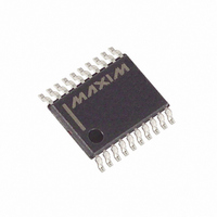
MAX1301BEUP+ Maxim Integrated Products, MAX1301BEUP+ Datasheet - Page 2

MAX1301BEUP+
Manufacturer Part Number
MAX1301BEUP+
Description
IC ADC 16BIT SER 4CH LP 20TSSOP
Manufacturer
Maxim Integrated Products
Datasheet
1.MAX1301BEUPT.pdf
(32 pages)
Specifications of MAX1301BEUP+
Number Of Bits
16
Sampling Rate (per Second)
115k
Data Interface
MICROWIRE™, QSPI™, Serial, SPI™
Number Of Converters
1
Power Dissipation (max)
105.5mW
Voltage Supply Source
Analog and Digital
Operating Temperature
-40°C ~ 85°C
Mounting Type
Surface Mount
Package / Case
20-TSSOP
Lead Free Status / RoHS Status
Lead free / RoHS Compliant
ABSOLUTE MAXIMUM RATINGS
8- and 4-Channel, ±3 x V
Serial 16-Bit ADCs
AV DD1 to AGND1 ....................................................-0.3V to +6V
AV DD2 to AGND2 ....................................................-0.3V to +6V
DV DD to DGND ........................................................-0.3V to +6V
DV DDO to DGNDO ..................................................-0.3V to +6V
DV DD to DV DDO ......................................................-0.3V to +6V
DV DD , DV DDO to AV DD1 ........................................-0.3V to +6V
AV DD1 , DV DD , DV DDO to AV DD2 ..........................-0.3V to +6V
DGND, DGNDO, AGND3, AGND2 to AGND1 ......-0.3V to +0.3V
CS, SCLK, DIN, DOUT, SSTRB to
Stresses beyond those listed under “Absolute Maximum Ratings” may cause permanent damage to the device. These are stress ratings only, and functional
operation of the device at these or any other conditions beyond those indicated in the operational sections of the specifications is not implied. Exposure to
absolute maximum rating conditions for extended periods may affect device reliability.
ELECTRICAL CHARACTERISTICS
(AV
external clock mode, V
(±3 x V
2
DC ACCURACY (Notes 1, 2)
Resolution
Integral Nonlinearity
Differential Nonlinearity
Transition Noise
Offset Error
Channel-to-Channel Gain
Matching
Channel-to-Channel Offset Error
Matching
Offset Temperature Coefficient
Gain Error
Gain Temperature Coefficient
DYNAMIC SPECIFICATIONS f
Signal-to-Noise Plus Distortion
DGNDO ............................................-0.3V to (DV DDO + 0.3V)
DD1
_______________________________________________________________________________________
REF
= AV
PARAMETER
), C
DD2
DOUT
= DV
= 50pF, C
DD
REF
= DV
= 4.096V (external reference operation), REFCAP = AV
SSTRB
IN(SINE-WAVE)
DDO
= 50pF, T
= 5V, AGND1 = DGND = DGNDO = AGND2 = AGND3 = 0, f
SYMBOL
SINAD
DNL
INL
A
= 5kHz, V
= -40°C to +85°C, unless otherwise noted. Typical values are at T
MAX130_A
MAX130_B
No missing codes
External or internal reference
Single-ended inputs
Differential inputs (Note 3)
Unipolar or bipolar
Unipolar or bipolar
Unipolar
Bipolar
Unipolar
Fully differential
Bipolar
Unipolar
Bipolar
Differential inputs, FSR = ±6 x V
Single-ended inputs, FSR = ±3 x V
Single-ended inputs, FSR = (±3 x V
Single-ended inputs, FSR = (±3 x V
IN
= FSR - 0.05dB, f
CONDITIONS
REF
CH0–CH7 to AGND1 .........................................-16.5V to +16.5V
REF, REFCAP to AGND1.......................-0.3V to (AV DD1 + 0.3V)
Continuous Current (any pin) ...........................................±50mA
Continuous Power Dissipation (T
Operating Temperature Range ...........................-40°C to +85°C
Junction Temperature .....................................................+150°C
Storage Temperature Range .............................-65°C to +150°C
Lead Temperature (soldering, 10s) .................................+300°C
20-Pin TSSOP (derate 11mW/°C above +70°C) ..........879mW
24-Pin TSSOP (derate 12.2mW/°C above +70°C) .......976mW
SAMPLE
Unipolar
Bipolar
Bipolar
Multirange Inputs,
REF
DD1
REF
= 130ksps (Notes 1, 2)
REF
REF
, maximum single-ended bipolar input range
)/2
)/4
MIN
16
80
-1
CLK
A
= +70°C)
= 3.5MHz (50% duty cycle),
0.025
±1.0
±1.0
TYP
-1.0
-2.0
1.0
1.5
1.0
10
91
89
86
83
1
0
5
A
= +25°C.)
MAX
±0.5
±0.8
±20
±10
±20
±2
±4
+2
±1
LSB
ppm/°C
ppm/°C
UNITS
%FSR
%FSR
Bits
LSB
LSB
mV
mV
dB
RMS


