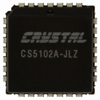
CS5102A-JLZ Cirrus Logic Inc, CS5102A-JLZ Datasheet - Page 19

CS5102A-JLZ
Manufacturer Part Number
CS5102A-JLZ
Description
IC ADC 16BIT 100/20KHZ 28-PLCC
Manufacturer
Cirrus Logic Inc
Datasheet
1.CS5101A-BL8Z.pdf
(39 pages)
Specifications of CS5102A-JLZ
Number Of Bits
16
Sampling Rate (per Second)
20k
Data Interface
Serial
Number Of Converters
1
Power Dissipation (max)
65mW
Voltage Supply Source
Analog and Digital, Dual ±
Operating Temperature
0°C ~ 70°C
Mounting Type
Surface Mount
Package / Case
28-PLCC
Lead Free Status / RoHS Status
Lead free / RoHS Compliant
Other names
598-1080-5
Available stocks
Company
Part Number
Manufacturer
Quantity
Price
Company:
Part Number:
CS5102A-JLZ
Manufacturer:
Cirrus Logic Inc
Quantity:
10 000
Part Number:
CS5102A-JLZ
Manufacturer:
CRYSTAL
Quantity:
20 000
4.5
The reference voltage directly defines the input
voltage range in both the unipolar and bipolar con-
figurations.
(BP/UP low), the first code transition occurs
0.5 LSB above AGND, and the final code transition
occurs 1.5 LSBs below VREF. In the bipolar con-
figuration (BP/UP high), the first code transition oc-
4.6
The CS5101A and CS5102A can be configured in
three different output modes, as well as an internal,
synchronous loop-back mode. This allows great
flexibility for design into a wide variety of systems.
The operating mode is selected by setting the
When SCKMOD is high, SCLK is an input, allowing
the data to be clocked out with an external serial
clock at rates up to 5 MHz. Additional clock edges
after #16 will clock out logic 1s on SDATA. Tying
SCKMOD low reconfigures SCLK as an output,
and the converter clocks out each bit as it is deter-
mined during the conversion process, at a rate of
1/4 the master clock speed. Table 2 shows an
overview of the different states of SCKMOD and
OUTMOD, and the corresponding output modes.
DS45F6
Analog Input Range/Coding Format
Output Mode Control
Unipolar Input Voltage
MODE
PDT
RBT
SSC
FRN
(VREF/2)-0.5 LSB
>(VREF-1.5 LSB)
VREF-1.5 LSB
<(+0.5 LSB)
+0.5 LSB
In
the
SCKMOD
unipolar
1
1
0
0
Binary
Offset
configuration
FFFF
FFFF
FFFE
7FFF
8000
0001
0000
0000
Table 2. Output Mode Control
OUTMOD
Table 1. Output Coding
1
0
1
0
Complement
curs 0.5 LSB above -VREF and the last transition
occurs 1.5 LSBs below +VREF. The CS5101A and
CS5102A can output data in either 2's comple-
ment, or binary format. If the CODE pin is high, the
output is in 2's complement format with a range of
-32,768 to +32,767. If the CODE pin is low, the out-
put is in binary format with a range of 0 to +65,535.
See Table 1 for output coding.
states of the SCKMOD and OUTMOD pins. In all
modes, data is output on SDATA, starting with the
MSB. Each subsequent data bit is updated on the
falling edge of SCLK.
4.6.1
PDT mode is selected by tying both SCKMOD and
OUTMOD high. In PDT mode, the SCLK pin is an
input. Data is registered during conversion, and
output during the following conversion cycle.
HOLD must be brought low, initiating another con-
version, before data from the previous conversion
is available on SDATA. If all the data has not been
clocked out before the next falling edge of HOLD,
the old data will be lost (Figure 5).
Two’s
7FFF
7FFF
7FFE
FFFF
SCLK
0000
8001
8000
8000
Output
Output
Input
Input
Pipelined Data Transmission
CH1/2
Output
Input
Input
Input
CS5101A CS5102A
Bipolar Input Voltage
<(-VREF+0.5 LSB)
>(VREF-1.5 LSB)
-VREF+0.5 LSB
VREF-1.5 LSB
-0.5 LSB
HOLD
Input
Input
Input
X
19


