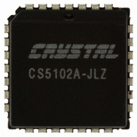
CS5102A-JLZ Cirrus Logic Inc, CS5102A-JLZ Datasheet - Page 22

CS5102A-JLZ
Manufacturer Part Number
CS5102A-JLZ
Description
IC ADC 16BIT 100/20KHZ 28-PLCC
Manufacturer
Cirrus Logic Inc
Datasheet
1.CS5101A-BL8Z.pdf
(39 pages)
Specifications of CS5102A-JLZ
Number Of Bits
16
Sampling Rate (per Second)
20k
Data Interface
Serial
Number Of Converters
1
Power Dissipation (max)
65mW
Voltage Supply Source
Analog and Digital, Dual ±
Operating Temperature
0°C ~ 70°C
Mounting Type
Surface Mount
Package / Case
28-PLCC
Lead Free Status / RoHS Status
Lead free / RoHS Compliant
Other names
598-1080-5
Available stocks
Company
Part Number
Manufacturer
Quantity
Price
Company:
Part Number:
CS5102A-JLZ
Manufacturer:
Cirrus Logic Inc
Quantity:
10 000
Part Number:
CS5102A-JLZ
Manufacturer:
CRYSTAL
Quantity:
20 000
5. SYSTEM DESIGN USING THE CS5101A & CS5102A
Figure 9 shows a general system connection diagram for the CS5101A and CS5102A.
5.1
Upon power up, the CS5101A and CS5102A must
be reset to guarantee a consistent starting condi-
tion and to initially calibrate the device. Due to
each device's low power dissipation and low tem-
perature drift, no warm-up time is required before
reset to accommodate any self-heating effects.
However, the voltage reference input should have
stabilized to within 0.25% of its final value before
RST rises to guarantee an accurate calibration.
Later, the CS5101A and CS5102A may be reset at
any time to initiate a single full calibration.
When RST is brought low all internal logic clears.
When RST returns high on the CS5101A, a cali-
bration cycle begins which takes 11,528,160 mas-
ter clock cycles to complete (approximately
22
System Initialization
S /(N + D ) pe rform an c e.
* Fo r b e st d y n a m ic
S o urce s
A n a log
V o lta g e R e fere n c e
M od e C on tro l
Figure 9. CS5101A/CS5102A System Connection Diagram
+ 5 V A
-5 V A
V D +
50
50
1 nF
1 nF
+
*
*
4.7 µ F
0.1 µ F
C0G
C0G
N P O
N P O
+
18
27
17
16
20
22
19
24
21
4.7 µ F
O U T M O D
S C K M O D
C O D E
V R E F
A G N D
A IN 1
A IN 2
R E F B U F
0.1 µ F
B P /U P
V A +
V A -
25
C S5101A
C S5102A
23
0.1 µ F
O R
10
10
26
TST
V D +
V D -
S S H /S D L
C R S /F IN
7
1
0.1 µ F
S D A T A
SLEEP
C L K IN
D G N D
C H 1 /2
X O U T
H O L D
STBY
S C L K
T R K 1
T R K 2
R S T
1.4 seconds with an 8 MHz master clock). The cal-
ibration cycle on the CS5102A takes 2,882,040
master clock cycles to complete (approximately
1.8 seconds with a 1.6 MHz master clock). The
CS5101A's and CS5102A's STBY output remains
low throughout the calibration sequence, and a ris-
ing transition indicates the device is ready for nor-
mal operation. While calibrating, the CS5101A and
CS5102A will ignore changes on the HOLD input.
To perform the reset function, a simple power-on
reset circuit can be built using a resistor and ca-
pacitor as shown in Figure 10. The resistor should
be less than or equal to 10 kΩ. The system power
supplies, voltage reference, and clock should all be
established prior RST rising.
0.1 µ F
+
28
13
10
12
11
14
15
4
3
2
5
8
9
6
XTAL
1 µ F
+
1 µ F
U nu se d Lo g ic in p uts s ho uld
b e tie d to V D + o r D G N D .
Interfa ce
C o n tro l
L og ic
D a ta
10 M
C 1
P D T, R B T ,
S S C
P D T, R B T ,
S S C
C 2 = C 1
C S 5 1 0 1 A
C S 5 1 0 2 A
C LO C K
EXT
CS5101A CS5102A
XTA L & C1 Table
F R N
F R N
8 .1 9 2 M H z
8 .0 M H z
1 .6 M H z
1 .6 M H z
2 .0 M H z
XTAL
or
C 1 , C 2
10 pF
10 pF
30 pF
30 pF
DS45F6


