MCP4728-E/UN Microchip Technology, MCP4728-E/UN Datasheet - Page 3
MCP4728-E/UN
Manufacturer Part Number
MCP4728-E/UN
Description
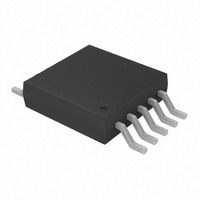
IC DAC 12BIT W/I2C 10-MSOP
Manufacturer
Microchip Technology
Specifications of MCP4728-E/UN
Number Of Converters
4
Settling Time
6µs
Package / Case
10-MSOP, Micro10™, 10-uMAX, 10-uSOP
Number Of Bits
12
Data Interface
I²C
Voltage Supply Source
Single Supply
Operating Temperature
-40°C ~ 125°C
Mounting Type
Surface Mount
Number Of Dac Outputs
4
Resolution
12 bit
Interface Type
I2C
Supply Voltage (max)
5.5 V
Supply Voltage (min)
2.7 V
Maximum Operating Temperature
+ 125 C
Mounting Style
SMD/SMT
Minimum Operating Temperature
- 40 C
Supply Current
110 mA
Voltage Reference
2.048 V
Lead Free Status / RoHS Status
Lead free / RoHS Compliant
For Use With
MCP4728EV - BOARD EVAL 12BIT 4CH DAC MCP4728
Power Dissipation (max)
-
Lead Free Status / Rohs Status
Lead free / RoHS Compliant
Available stocks
Company
Part Number
Manufacturer
Quantity
Price

Part Number:
MCP4728-E/UN
Manufacturer:
MICROCHIP/微芯
Quantity:
20 000


1.0
Absolute Maximum Ratings†
V
All inputs and outputs w.r.t V
Current at Input Pins ....................................................±2 mA
Current at Supply Pins ............................................. ±110 mA
Current at Output Pins ...............................................±25 mA
Storage Temperature ...................................-65°C to +150°C
Ambient Temp. with Power Applied .............-55°C to +125°C
ESD protection on all pins ................ ≥ 4 kV HBM, ≥ 400V MM
Maximum Junction Temperature (T
ELECTRICAL CHARACTERISTICS
© 2010 Microchip Technology Inc.
Electrical Specifications: Unless otherwise indicated, all parameters apply at V
R
Power Requirements
Operating Voltage
Supply Current with
External Reference
(V
(Note
Power-Down Current with
External Reference
Supply Current with
Internal Reference
(V
(Note
Power-Down Current with
Internal Reference
Note 1:
DD
L
REF
REF
...................................................................................6.5V
= 5 kΩ, C
= V
1)
= Internal)
1)
2:
3:
4:
5:
6:
7:
8:
9:
Parameter
ELECTRICAL
CHARACTERISTICS
DD
All digital input pins (SDA, SCL, LDAC) are tied to “High”, Output pins are unloaded, code = 0 x 000.
The power-up ramp rate measures the rise of V
This parameter is ensured by design and not 100% tested.
This parameter is ensured by characterization and not 100% tested.
Test code range: 100 - 4000 codes, V
Time delay to settle to a new reference when switching from external to internal reference or vice versa.
This parameter is indirectly tested by Offset and Gain error testing.
Within 1/2 LSB of the final value when code changes from 1/4 of to 3/4 of full scale.
This time delay is measured from the falling edge of ACK pulse in I
This time delay is not included in the output settling time specification.
)
L
= 100 pF, G
SS
X
................. -0.3V to V
= 1, T
Symbol
I
I
I
I
J
DD_EXT
PD_EXT
DD_INT
PD_INT
) ......................... +150°C
V
DD
A
= -40°C to +125°C. Typical values are at +25°C, V
Min
2.7
—
—
—
—
—
—
—
—
—
—
DD
+0.3V
REF
Typical
= V
800
600
400
200
800
600
400
200
40
45
DD
DD
, V
DD
over time.
1400
1400
†
ratings” may cause permanent damage to the device. This is
a stress rating only and functional operation of the device at
these or any other conditions above those indicated in the
operation listings of this specification is not implied. Exposure
to maximum rating conditions for extended periods may affect
device reliability.
Max
5.5
60
—
—
—
—
—
—
—
= 5.5V.
Notice: Stresses above those listed under “Maximum
Units
µA
µA
µA
µA
µA
µA
µA
µA
µA
nA
V
2
C command to the beginning of V
DD
V
All 4 channels are in Normal mode.
3 channels are in Normal mode,
1 channel is powered down.
2 channels are in Normal mode,
2 channel are powered down.
1 channel is in Normal mode,
3 channels are powered down.
All 4 channels are powered down.
(V
V
V
All 4 channels are in normal mode.
3 channels are in Normal mode,
1 channel is powered down.
2 channels are in Normal mode,
2 channels are powered down.
1 channel is in Normal mode,
3 channels are powered down.
All 4 channels are powered down.
V
REF
REF
DD
REF
REF
= +2.7V to 5.5V, V
IH
= 5.5V
= V
= Internal Reference
= Internal Reference
= V
= V
DD
DD
DD
MCP4728
Conditions
, V
, V
)
DD
IL
= V
= 5.5V
DS22187E-page 3
SS.
SS
= 0V,
OUT
.
Related parts for MCP4728-E/UN
Image
Part Number
Description
Manufacturer
Datasheet
Request
R

Part Number:
Description:
12-bit, Quad Digital-to-analog Converter With Eeprom Memory
Manufacturer:
Microchip Technology Inc.
Datasheet:
Part Number:
Description:
Manufacturer:
Microchip Technology Inc.
Datasheet:
Part Number:
Description:
Manufacturer:
Microchip Technology Inc.
Datasheet:
Part Number:
Description:
Manufacturer:
Microchip Technology Inc.
Datasheet:
Part Number:
Description:
Manufacturer:
Microchip Technology Inc.
Datasheet:
Part Number:
Description:
Manufacturer:
Microchip Technology Inc.
Datasheet:
Part Number:
Description:
Manufacturer:
Microchip Technology Inc.
Datasheet:
Part Number:
Description:
Manufacturer:
Microchip Technology Inc.
Datasheet:
Part Number:
Description:
Manufacturer:
Microchip Technology Inc.
Datasheet: