MCP4728-E/UN Microchip Technology, MCP4728-E/UN Datasheet - Page 52
MCP4728-E/UN
Manufacturer Part Number
MCP4728-E/UN
Description
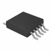
IC DAC 12BIT W/I2C 10-MSOP
Manufacturer
Microchip Technology
Specifications of MCP4728-E/UN
Number Of Converters
4
Settling Time
6µs
Package / Case
10-MSOP, Micro10™, 10-uMAX, 10-uSOP
Number Of Bits
12
Data Interface
I²C
Voltage Supply Source
Single Supply
Operating Temperature
-40°C ~ 125°C
Mounting Type
Surface Mount
Number Of Dac Outputs
4
Resolution
12 bit
Interface Type
I2C
Supply Voltage (max)
5.5 V
Supply Voltage (min)
2.7 V
Maximum Operating Temperature
+ 125 C
Mounting Style
SMD/SMT
Minimum Operating Temperature
- 40 C
Supply Current
110 mA
Voltage Reference
2.048 V
Lead Free Status / RoHS Status
Lead free / RoHS Compliant
For Use With
MCP4728EV - BOARD EVAL 12BIT 4CH DAC MCP4728
Power Dissipation (max)
-
Lead Free Status / Rohs Status
Lead free / RoHS Compliant
Available stocks
Company
Part Number
Manufacturer
Quantity
Price

Part Number:
MCP4728-E/UN
Manufacturer:
MICROCHIP/微芯
Quantity:
20 000


MCP4728
7.1.1
The user can test the presence of the MCP4728 device
on the I
conversion. This test can be achieved by checking an
acknowledge response from the MCP4728 device after
sending a read or write command.
example with a read command:
a.
b.
c.
FIGURE 7-2:
7.2
Inductively-coupled AC transients and digital switching
noise from other devices can affect DAC performance
and DAC output signal integrity. Careful board layout
will minimize these effects. Bench testing has shown
that a multi-layer board utilizing a low-inductance
ground plane, isolated inputs, isolated outputs and
proper decoupling are critical to achieving good DAC
performance.
Separate digital and analog ground planes are
recommended. In this case, the V
pins of the V
terminated to the analog ground plane.
DS22187E-page 52
SDA
SCL
Set the R/W bit “High” or “Low” in the address
byte.
Check the ACK pulse after sending the address
byte.
If the device acknowledges (ACK = 0) the
command, then the device is connected,
otherwise it is not connected.
Send Stop Bit.
Start
Bit
Layout Considerations
2
C bus line without performing a data
DEVICE CONNECTION TEST
DD
1
1
Device Code
capacitors of the MCP4728 should be
2
1 0
3
I
2
Address Byte
C Bus Connection Test.
4
1 A2 A1 A0 1
Address bits
5
6
SS
Figure 7-2
7
pin and the ground
8
R/W
9
MCP4728
Response
shows an
Stop
Bit
7.3
The power source should be as clean as possible. The
power supply to the device is used for both V
DAC voltage reference by selecting V
noise induced on the V
performance. A typical application will require a bypass
capacitor in order to filter out high-frequency noise on
the V
supply’s traces or as a result of changes on the DAC
output. The bypass capacitor helps to minimize the
effect of these noise sources on signal integrity.
Figure 7-1
capacitors (a 10 µF tantalum capacitor and a 0.1 µF
ceramic capacitor) in parallel on the V
capacitors should be placed as close to the V
possible (within 4 mm). If the application circuit has
separate digital and analog power supplies, the V
and V
the analog plane.
7.4
The device consumes very little power when it is in
Power-Down
Power-Down mode, most circuits in the selected
channel are turned off. It is recommended to power
down any unused channel.
The device consumes the least amount of power if it
enters the Power-Down mode after the internal voltage
reference is disabled. This can be achieved by
selecting V
channels, and then issuing the Power-Down mode for
all channels.
7.5
The user can store the I
configuration bits and DAC input code of each channel
in the on-board nonvolatile EEPROM memory using
the I
readable and writable using the I
When the MCP4728 device is first powered-up or
receives General Call Reset Command, it uploads the
EEPROM contents to the DAC output registers
automatically and provides analog outputs immediately
with the saved settings in EEPROM. This feature is
very useful in applications where the MCP4728 device
is used to provide set points or calibration data for other
devices in the application systems. The MCP4728
device can save important system parameters when
the application system experiences power failure. See
Section 5.5 “Writing and Reading Registers and
EEPROM”
EEPROM memory.
2
DD
C write command. The contents of EEPROM are
SS
line. The noise can be induced onto the power
pins of the MCP4728 device should reside on
Power Supply Considerations
Using Power Saving Feature
Using Nonvolatile EEPROM
Memory
shows an example of using two bypass
for more details on using the nonvolatile
DD
(shut-down)
as the voltage reference for all 4
© 2010 Microchip Technology Inc.
DD
2
C device address bits,
mode.
line can affect DAC
2
C command.
REF
DD
During
= V
line. These
DD
DD.
DD
pin as
Any
and
the
DD
Related parts for MCP4728-E/UN
Image
Part Number
Description
Manufacturer
Datasheet
Request
R

Part Number:
Description:
12-bit, Quad Digital-to-analog Converter With Eeprom Memory
Manufacturer:
Microchip Technology Inc.
Datasheet:
Part Number:
Description:
Manufacturer:
Microchip Technology Inc.
Datasheet:
Part Number:
Description:
Manufacturer:
Microchip Technology Inc.
Datasheet:
Part Number:
Description:
Manufacturer:
Microchip Technology Inc.
Datasheet:
Part Number:
Description:
Manufacturer:
Microchip Technology Inc.
Datasheet:
Part Number:
Description:
Manufacturer:
Microchip Technology Inc.
Datasheet:
Part Number:
Description:
Manufacturer:
Microchip Technology Inc.
Datasheet:
Part Number:
Description:
Manufacturer:
Microchip Technology Inc.
Datasheet:
Part Number:
Description:
Manufacturer:
Microchip Technology Inc.
Datasheet: