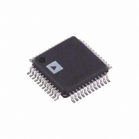
AD9763ASTZ Analog Devices Inc, AD9763ASTZ Datasheet - Page 13

AD9763ASTZ
Manufacturer Part Number
AD9763ASTZ
Description
IC DAC 10BIT DUAL 125MSPS 48LQFP
Manufacturer
Analog Devices Inc
Series
TxDAC+®r
Specifications of AD9763ASTZ
Data Interface
Parallel
Settling Time
35ns
Number Of Bits
10
Number Of Converters
2
Voltage Supply Source
Analog and Digital
Power Dissipation (max)
450mW
Operating Temperature
-40°C ~ 85°C
Mounting Type
Surface Mount
Package / Case
48-LQFP
Resolution (bits)
10bit
Sampling Rate
125MSPS
Input Channel Type
Parallel
Supply Voltage Range - Analog
3V To 5.5V
Supply Voltage Range - Digital
2.7V To 5.5V
Lead Free Status / RoHS Status
Lead free / RoHS Compliant
For Use With
AD9763-EBZ - BOARD EVAL FOR AD9763
Lead Free Status / RoHS Status
Lead free / RoHS Compliant, Lead free / RoHS Compliant
Available stocks
Company
Part Number
Manufacturer
Quantity
Price
Company:
Part Number:
AD9763ASTZ
Manufacturer:
ADI
Quantity:
180
Company:
Part Number:
AD9763ASTZ
Manufacturer:
Analog Devices Inc
Quantity:
10 000
Part Number:
AD9763ASTZ
Manufacturer:
ADI/亚德诺
Quantity:
20 000
Company:
Part Number:
AD9763ASTZRL
Manufacturer:
Analog Devices Inc
Quantity:
10 000
Part Number:
AD9763ASTZRL
Manufacturer:
ADI/亚德诺
Quantity:
20 000
ADDITIONAL
The full-scale output current of each DAC is regulated by
separate reference control amplifiers and can be set from 2 mA
to 20 mA via an external resistor (R
scale adjust (FSADJ) pin. The external resistor, in combination
with both the reference control amplifier and voltage reference
(V
the segmented current sources with the proper scaling factor.
The full-scale current (I
REFERENCE OPERATION
The AD9763 contains an internal 1.20 V band gap reference.
This can easily be overridden by an external reference with no
effect on performance. REFIO serves as either an input or
output, depending on whether the internal or an external
reference is used. To use the internal reference, simply decouple
the REFIO pin to ACOM with a 0.1 μF capacitor. The internal
reference voltage is present at REFIO. If the voltage at REFIO is
used elsewhere in the circuit, an external buffer amplifier with
an input bias current of less than 100 nA should be used. An
example of the use of the internal reference is shown in Figure 23.
An external reference can be applied to REFIO, as shown in
Figure 24. The external reference provides either a fixed
reference voltage to enhance accuracy and drift performance or
a varying reference voltage for gain control. The 0.1 μF compen-
sation capacitor is not required because the internal reference is
overridden, and the relatively high input impedance of REFIO
minimizes any loading of the external reference.
EXTERNAL
REFIO
REFERENCE
LOAD
EXTERNAL
REFERENCE
EXTERNAL
OPTIONAL
), sets the reference current (I
AVDD
BUFFER
Figure 24. External Reference Configuration
Figure 23. Internal Reference Configuration
I
REF
0.1µF
I
REF
2kΩ
OUTFS
2kΩ
REFIO
FSADJ
GAINCTRL
) is 32 × I
1.2V
REF
REFIO
FSADJ
GAINCTRL
1.2V
REF
SET
REF
REF
) connected to the full
REFERENCE
), which is replicated to
AD9763
SECTION
.
REFERENCE
AD9763
SECTION
CURRENT
SOURCE
ARRAY
AVDD
CURRENT
SOURCE
ARRAY
ACOM
AVDD
ACOM
Rev. D | Page 13 of 32
GAIN CONTROL MODE
The AD9763 allows the gain of each channel to be independ-
ently set by connecting one R
R
cost, a single R
channels simultaneously.
When GAINCTRL is low (connected to AGND), the independ-
ent channel gain control mode using two resistors is enabled. In
this mode, individual R
FSADJ1 and FSADJ2. When GAINCTRL is high (connected to
AVDD), the master/slave channel gain control mode using one
resistor is enabled. In this mode, a single R
to FSADJ1 and the resistor on FSADJ2 must be removed.
Note that only parts with a date code of 9930 or later have the
master/slave gain control function. For parts with a date code
before 9930, Pin 42 must be connected to AGND, and the part
operates in the two-resistor, independent gain control mode.
REFERENCE CONTROL AMPLIFIER
Both of the DACs in the AD9763 contain a control amplifier
that is used to regulate the full-scale output current (I
control amplifier is configured as a V-I converter as shown in
Figure 23, so that its current output (I
ratio of the V
Equation 4. I
the proper scale factor to set I
The control amplifier allows a wide (10:1) adjustment span of
I
625 μA. The wide adjustment range of I
benefits. The first relates directly to the power dissipation of the
AD9763, which is proportional to I
Dissipation section). The second relates to the 20 dB adjustment,
useful for system gain control purposes.
The small signal bandwidth of the reference control amplifier is
approximately 500 kHz and can be used for low frequency,
small signal multiplying applications.
DAC TRANSFER FUNCTION
Both DACs in the AD9763 provide complementary current
outputs, I
output (I
while I
The current output appearing at I
both the input code and I
where DAC CODE = 0 to 1023 (decimal representation).
OUTFS
SET
resistor to FSADJ2. To add flexibility and reduce system
I
I
OUTA
OUTB
from 2mA to 20 mA by setting I
OUTB
OUTFS
OUTA
= (1023 − DAC CODE/1024) × I
= (DAC CODE/1024) × I
, the complementary output, provides no current.
REF
REFIO
) when all bits are high (DAC CODE = 1023)
and I
SET
is copied to the segmented current sources with
resistor can be used to set the gain of both
and an external resistor (R
OUTB
. I
B
SET
OUTA
OUTFS
resistors should be connected to
SET
OUTFS
provides a near full-scale current
and can be expressed as
resistor to FSADJ1 and another
OUTA
as stated in Equation 3.
OUTFS
OUTFS
REF
REF
and I
OUTFS
) is determined by the
(refer to the Power
between 62.5 μA and
SET
OUTFS
OUTB
SET
provides several
resistor is connected
) as stated in
is a function of
AD9763
OUTFS
). The
(1)
(2)


