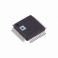
AD9763ASTZ Analog Devices Inc, AD9763ASTZ Datasheet - Page 22

AD9763ASTZ
Manufacturer Part Number
AD9763ASTZ
Description
IC DAC 10BIT DUAL 125MSPS 48LQFP
Manufacturer
Analog Devices Inc
Series
TxDAC+®r
Specifications of AD9763ASTZ
Data Interface
Parallel
Settling Time
35ns
Number Of Bits
10
Number Of Converters
2
Voltage Supply Source
Analog and Digital
Power Dissipation (max)
450mW
Operating Temperature
-40°C ~ 85°C
Mounting Type
Surface Mount
Package / Case
48-LQFP
Resolution (bits)
10bit
Sampling Rate
125MSPS
Input Channel Type
Parallel
Supply Voltage Range - Analog
3V To 5.5V
Supply Voltage Range - Digital
2.7V To 5.5V
Lead Free Status / RoHS Status
Lead free / RoHS Compliant
For Use With
AD9763-EBZ - BOARD EVAL FOR AD9763
Lead Free Status / RoHS Status
Lead free / RoHS Compliant, Lead free / RoHS Compliant
Available stocks
Company
Part Number
Manufacturer
Quantity
Price
Company:
Part Number:
AD9763ASTZ
Manufacturer:
ADI
Quantity:
180
Company:
Part Number:
AD9763ASTZ
Manufacturer:
Analog Devices Inc
Quantity:
10 000
Part Number:
AD9763ASTZ
Manufacturer:
ADI/亚德诺
Quantity:
20 000
Company:
Part Number:
AD9763ASTZRL
Manufacturer:
Analog Devices Inc
Quantity:
10 000
Part Number:
AD9763ASTZRL
Manufacturer:
ADI/亚德诺
Quantity:
20 000
AD9763
I and Q digital data can be fed into the AD9763 in two different
ways. In dual port mode, the Digital I information drives one
input port, while the Digital Q information drives the other
input port. If no interpolation filter precedes the DAC, the
symbol rate is the rate that the system clock drives the CLK and
WRT pins on the AD9763. In interleaved mode, the digital
input stream at Port 1 contains the I and the Q information in
alternating digital words. Using IQSEL and IQRESET, the
AD9763 can be synchronized to the I and Q data stream. The
internal timing of the AD9763 routes the selected I and Q data
to the correct DAC output. In interleaved mode, if no inter-
polation filter precedes the AD9763, the symbol rate is half that
of the system clock driving the digital data stream and the
IQWRT and IQCLK pins on the AD9763.
CDMA
Carrier division multiple access (CDMA) is an air transmit/
receive scheme where the signal in the transmit path is modu-
lated with a pseudorandom digital code (sometimes referred to
as the spreading code). The effect of this is to spread the trans-
mitted signal across a wide spectrum. Similar to a DMT waveform,
a CDMA waveform containing multiple subscribers can be
characterized as having a high peak-to-average ratio (crest factor),
thus demanding highly linear components in the transmit
signal path. The bandwidth of the spectrum is defined by the
CDMA standard being used, and in operation is implemented
by using a spreading code with particular characteristics.
Distortion in the transmit path can lead to power being trans-
mitted out of the defined band. The ratio of power transmitted
in-band to out-of-band is often referred to as adjacent channel
Rev. D | Page 22 of 32
power (ACP). This is a regulatory issue due to the possibility of
interference with other signals being transmitted by air. Regula-
tory bodies define a spectral mask outside of the transmit band,
and the ACP must fall under this mask. If distortion in the trans-
mit path causes the ACP to be above the spectral mask, then
filtering, or different component selection, is needed to meet
the mask requirements.
Figure 44 shows the AD9763, when used with the AD8346,
reconstructing a wideband CDMA signal at 2.4 GHz. The base-
band signal is being sampled at 65 MSPS and has a chip rate of
8 M chips.
–100
–110
–120
–130
–30
–40
–50
–60
–70
–80
–90
Recreated at 2.4 GHz, Adjacent Channel Power > 60 dBm
Figure 44. CDMA Signal, 8 M Chips Sampled at 65 MSPS,
CENTER 2.4GHz
==
c11
c11
C0
FREQUENCY
3MHz
cu1
C0
SPAN 30MHz
cu1


