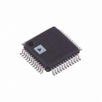
AD9763ASTZ Analog Devices Inc, AD9763ASTZ Datasheet - Page 7

AD9763ASTZ
Manufacturer Part Number
AD9763ASTZ
Description
IC DAC 10BIT DUAL 125MSPS 48LQFP
Manufacturer
Analog Devices Inc
Series
TxDAC+®r
Specifications of AD9763ASTZ
Data Interface
Parallel
Settling Time
35ns
Number Of Bits
10
Number Of Converters
2
Voltage Supply Source
Analog and Digital
Power Dissipation (max)
450mW
Operating Temperature
-40°C ~ 85°C
Mounting Type
Surface Mount
Package / Case
48-LQFP
Resolution (bits)
10bit
Sampling Rate
125MSPS
Input Channel Type
Parallel
Supply Voltage Range - Analog
3V To 5.5V
Supply Voltage Range - Digital
2.7V To 5.5V
Lead Free Status / RoHS Status
Lead free / RoHS Compliant
For Use With
AD9763-EBZ - BOARD EVAL FOR AD9763
Lead Free Status / RoHS Status
Lead free / RoHS Compliant, Lead free / RoHS Compliant
Available stocks
Company
Part Number
Manufacturer
Quantity
Price
Company:
Part Number:
AD9763ASTZ
Manufacturer:
ADI
Quantity:
180
Company:
Part Number:
AD9763ASTZ
Manufacturer:
Analog Devices Inc
Quantity:
10 000
Part Number:
AD9763ASTZ
Manufacturer:
ADI/亚德诺
Quantity:
20 000
Company:
Part Number:
AD9763ASTZRL
Manufacturer:
Analog Devices Inc
Quantity:
10 000
Part Number:
AD9763ASTZRL
Manufacturer:
ADI/亚德诺
Quantity:
20 000
PIN CONFIGURATION AND FUNCTION DESCRIPTIONS
Table 6. Pin Function Descriptions
Pin No.
1 to 10
11 to 14, 33 to 36
15, 21
16, 22
17
18
19
20
23 to 32
37
38
39, 40
41
42
43
44
45, 46
47
48
Name
DCOM1, DCOM2
DVDD1, DVDD2
WRT1/IQWRT
CLK1/IQCLK
CLK2/IQRESET
WRT2/IQSEL
SLEEP
ACOM
I
FSADJ2
GAINCTRL
REFIO
FSADJ1
I
AVDD
MODE
PORT1
NC
PORT2
OUTA2
OUTB1
, I
, I
OUTB2
OUTA1
NC = NO CONNECT
DB9P1 (MSB)
DB0P1 (LSB)
DB8P1
DB7P1
DB6P1
DB5P1
DB4P1
DB3P1
DB2P1
DB1P1
Description
Data Bit DB9P1 to Data Bit DB0P1.
No Connect.
Digital Common.
Digital Supply Voltage.
Input Write Signal. This is the input write signal for PORT 1; IQWRT in interleaving mode.
Clock Input. This is the clock input for DAC1; IQCLK in interleaving mode.
Clock Input. This is the clock input for DAC2; IQRESET in interleaving mode.
Input Write Signal. This is the input write signal for PORT 2; IQSEL in interleaving mode.
Data Bit DB9P2 to Data Bit DB0P2.
Power-Down Control Input.
Analog Common.
PORT 2 Differential DAC Current Outputs.
Full-Scale Current Output Adjust for DAC2.
Gain Control Mode. 0 = 2 resistor, 1 = 1 resistor.
Reference Input/Output.
Full-Scale Current Output Adjust for DAC1.
PORT 1 Differential DAC Current Outputs.
Analog Supply Voltage.
Mode Select. 1 = dual port, 0 = interleaved.
NC
NC
10
11
12
1
2
3
4
5
6
7
8
9
48 47 46 45 44 43 42 41 40 39 38 37
13 14 15 16 17 18 19 20 21 22 23 24
PIN 1
Figure 3. Pin Configuration
Rev. D | Page 7 of 32
(Not to Scale)
TOP VIEW
AD9763
36
35
34
33
32
31
30
29
28
27
26
25
NC
NC
NC
NC
DB0P2 (LSB)
DB1P2
DB2P2
DB3P2
DB4P2
DB5P2
DB6P2
DB7P2
AD9763


