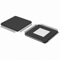
DAC1003D160HW/C1,5 NXP Semiconductors, DAC1003D160HW/C1,5 Datasheet - Page 6

DAC1003D160HW/C1,5
Manufacturer Part Number
DAC1003D160HW/C1,5
Description
IC DAC 10BIT 160MSPS 80-HTQFP
Manufacturer
NXP Semiconductors
Datasheet
1.DAC1003D160HWC11.pdf
(19 pages)
Specifications of DAC1003D160HW/C1,5
Settling Time
16ns
Number Of Bits
10
Data Interface
Parallel
Number Of Converters
2
Voltage Supply Source
Analog and Digital
Power Dissipation (max)
540mW
Operating Temperature
-40°C ~ 85°C
Mounting Type
Surface Mount
Package / Case
80-TQFP Exposed Pad, 80-eTQFP, 80-HTQFP, 80-VQFP
Lead Free Status / RoHS Status
Lead free / RoHS Compliant
Other names
935286682518
DAC1003D160HW/C1-T
DAC1003D160HW/C1-T
DAC1003D160HW/C1-T
DAC1003D160HW/C1-T
Available stocks
Company
Part Number
Manufacturer
Quantity
Price
Company:
Part Number:
DAC1003D160HW/C1,5
Manufacturer:
IDT, Integrated Device Technology Inc
Quantity:
10 000
NXP Semiconductors
7. Functional description
DAC1003D160_2
Product data sheet
Fig 3. Equivalent analog output circuit
IOUT/QOUT
The DAC1003D160 is a segmented architecture composed of a 7-bit thermometer
sub-DAC and the remaining 3-bit in a binary weighted sub-DAC.
The device produces two complementary current outputs on both channels, respectively
pins IOUT/IOUTN and QOUT/QOUTN which need to be connected via a load resistor to
the ground.
Figure 3
parallel combination of PMOS current sources and associated switches for each segment.
The cascade source configuration enables the increase of the output impedance of the
source and the improvement of the dynamic performance of the DAC by introducing less
distortion.
Figure 4
by the output of the internal regulator connected to the inverting input of the internal
operational amplifiers, while external resistors R
pins IVIRES and QVIRES. Thus the output current of the two DACs is typically fixed to
20 mA with an appropriate choice of these resistors. This configuration is optimal for
temperature drift compensation because the band gap can be matched with the voltage
on the feedback resistors.
The relation between full-scale output current I
The output current can also be adjusted by imposing an external reference voltage to the
inverting input pin GAPOUT and disabling the internal band gap with pin GAPD set to
HIGH. At a voltage lower than 1.2 V the current can be set at values lower than 20 mA.
The input references at pins IVIRES and QVIRES may also be driven by separate
reference voltages to adjust independently the two DAC currents.
R
I
AGND
=
R
L
2048 V
----------------------------------------- -
82
shows the equivalent analog output circuit of one DAC, which consists of a
shows the internal reference configuration. In this case the bias current is given
AGND
IOUTN/QOUTN
R
DAC1003D160
L
I
O FS
GAPOUT
014aaa537
Rev. 02 — 13 August 2008
Fig 4. Internal reference configuration
Dual 10 bits DAC, up to 160 MHz, 2 x interpolation
R
R
I
Q
GAPOUT
QVIRES
IVIRES
O(fs)
GAPD
AGND
I
and R
and the R
DAC1003D160
Q
are connected respectively to
BAND GAP
INTERNAL
DAC1003D160
I
(R
Q
) is:
© NXP B.V. 2008. All rights reserved.
I DAC current
sources array
Q DAC current
sources array
014aaa538
6 of 19


