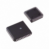
AD7568BP Analog Devices Inc, AD7568BP Datasheet - Page 12

AD7568BP
Manufacturer Part Number
AD7568BP
Description
IC DAC 12BIT LC2MOS OCTAL 44PLCC
Manufacturer
Analog Devices Inc
Datasheet
1.AD7568BPZ-REEL.pdf
(12 pages)
Specifications of AD7568BP
Mounting Type
Surface Mount
Rohs Status
RoHS non-compliant
Settling Time
500ns
Number Of Bits
12
Data Interface
Serial
Number Of Converters
8
Voltage Supply Source
Single Supply
Power Dissipation (max)
17.5mW
Operating Temperature
-40°C ~ 85°C
Package / Case
44-PLCC
Resolution (bits)
12bit
No. Of Pins
44
Peak Reflow Compatible (260 C)
No
Update Rate
2MSPS
No. Of Bits
12 Bit
Leaded Process Compatible
No
No. Of Outputs
8
Resolution
12-Bit
Lead Free Status / RoHS Status
Contains lead / RoHS non-compliant
Available stocks
Company
Part Number
Manufacturer
Quantity
Price
Company:
Part Number:
AD7568BPZ
Manufacturer:
Analog Devices Inc
Quantity:
135
Company:
Part Number:
AD7568BPZ
Manufacturer:
Analog Devices Inc
Quantity:
10 000
Part Number:
AD7568BPZ
Manufacturer:
ADI/亚德诺
Quantity:
20 000
Company:
Part Number:
AD7568BPZ-REEL
Manufacturer:
Analog Devices Inc
Quantity:
10 000
AD7568
For systems which contain larger numbers of AD7568s and
where the user also wishes to read back the DAC contents for
diagnostic purposes, the SDOUT pin may be used to daisy
chain several devices together and provide the necessary serial
readback. An example with the 68HC11 is shown in Figure 25.
The routine below shows how four AD7568s would be pro-
grammed in such a system. Data is transmitted at the MOSI pin
of the 68HC11. It flows through the input shift registers of the
AD7568s and finally appears at the SDOUT pin of DAC N. So,
the readback routine can be invoked any time after the first four
words have been transmitted (the four input shift registers in the
chain will now be filled up and further activity on the CLKIN
pin will result in data being read back to the microcomputer
through the MISO pin). System connectivity can be verified in
this manner. For a four-device system (32 DACs) a two-line to
four-line decoder is necessary.
Note that to program the 32 DACs, 35 transmit operations are
needed. In the routine, three words must be retransmitted. The
first word for DACs #3, #2 and #1 must be transmitted twice in
order to synchronize their arrival at the SDIN pin with A0 going
low.
Bring PC7 (FSIN) low to allow writing to the AD7568s.
Bring PC7 (FSIN) high to disable writing to the AD7568s.
Enable AD7568 #4 (Bring A0 low). Disable the others.
Enable AD7568 #3, Disable the others.
Enable AD7568 #2, Disable the others.
Enable AD7568 #1, Disable the others.
Table V. Routine for Loading 4 AD7568s Connected As in
Figure 25
Transmit 1st 16-bit word: Data for DAC H, #4
. . . .
. . . .
Transmit 9th 16-bit word: Data for DAC H, #3
Transmit 9th 16-bit word again: Data for DAC H, #3
Transmit 10th 16-bit word: Data for DAC G, #3
Transmit 11th 16-bit word: Data for DAC F, #3
Transmit 12th 16-bit word: Data for DAC E, #3
. . . .
. . . .
Transmit 17th 16-bit word: Data for DAC H, #2
Transmit 17th 16-bit word again: Data for DAC H, #2
Transmit 18th 16-bit word: Data for DAC G, #2
Transmit 19th 16-bit word: Data for DAC F, #2
. . . .
. . . .
Transmit 25th word: Data for DAC H, #1
Transmit 25th word again: Data for DAC H, #1
Transmit 26th word: Data for DAC G, #1
. . . .
. . . .
Transmit 32nd word: Data for DAC A, #1
–12–
0.079 + 0.004/–0.002
(2 + 0.1/–0.05)
0.031
(0.8
0.036
(0.92
0.394
*ADDITIONAL PINS OMITTED FOR CLARITY
(10
0.15)
DECODE LOGIC
0.006
0.004
0.1)
68HC11*
0.1)
0.004
Dimensions shown in inches and (mm).
Figure 25. Multi-DAC System
0.096 (2.45) MAX
OUTLINE DIMENSIONS
MOSI
MISO
SCK
PC7
PC6
44-Pin PQFP
0.036
(0.92
(Suffix S)
4
4
0.004
0.1)
34
44
0.014
(0.35
33
1
0.002
0.05)
PIN 1
0.394
0.547
(13.9
TOP VIEW
SDIN
FSIN
SCLK
LDAC
A0
FSIN
SCLK
LDAC
A0
FSIN
SCLK
LDAC
A0
(10
AD7568*
AD7568*
AD7568*
(DAC 1)
(DAC N)
(DAC 2)
0.004 SQ
SDOUT
SDOUT
SDOUT
0.01 SQ
SDIN
SDIN
0.25)
0.1)
0.031
(0.8
0.05)
0.002
23
11
12
22
REV. B


